
User guide
3
U2745B
4734A–RKE–11/03
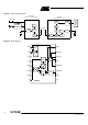
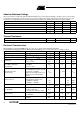
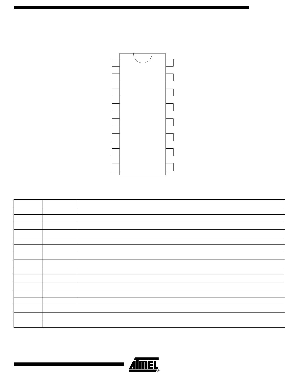
Pin Configuration
Figure 3. Pinning SSO16
VCC
CLK
GND
LFVCC
LFGND
LF
ASK
EN
1
2
3
4
5
6
7
8
16
15
14
13
12
11
10
9
PWRVCC
ANT
PWRGND1
PWRGND2
XTO1
NC
GND
PWRSET
U2745B
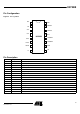
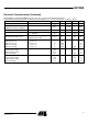
Pin Description
Pin Symbol Function
1 ASK Modulation input ASK
2 EN Enable input
3 VCC Supply voltage
4 CLK Clock output
5 GND Ground
6 LFVCC Supply voltage VCO
7 LFGND VCO ground
8 LF Circuit PLL loop
9 NC Not connected
10 XTO1 Connection for crystal
11 PWRGND2 Power GND2
12 PWRGND1 Power GND1
13 ANT RF output
14 PWRVCC Supply voltage power amplifier
15 PWRSET Applied to VCC
16 GND Ground