
User guide

7
U2741B
4733A–RKE–11/03
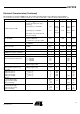
Oscillator frequency XTO
M-version: at T
amb
= 25°C
N-version: full temperature range
(monitoring)
Crystal frequency = 13.56 MHz
Crystal frequency = 6.78 MHz
Load capacity of the crystal must be
selected accordingly
f
XTO
f
XTO
13.56 -
30 ppm
6.78 -
30 ppm
13.56
6.78
13.56 +
30 ppm
6.78 +
30 ppm
MHz
MHz
Loop bandwidth
For best LO noise
Loop filter components:
C
2
= 3.9 nF, C
1
= 15 nF, R
4
= 220 W
B
Loop
100 kHz
Phase noise PLL
Referring to the phase comparator
f
PC
= 6.78 MHz
PN
PLL
-111 -105 dBC/Hz
Phase noise VCO
at 1 MHz
at 36 MHz
PN
VCO
PN
VCO
-91
-123
-87
-119
dBC/Hz
Frequency range of the VCO f
VCO
300 450 MHz
Clock output
(CMOS microcontroller compatible)
Clk
out
f
out
/128 MHz
Load capacitance at CLK C
CLK
10 pF
Series resonance R of the crystal
f
XTO
= 13.56 MHz
f
XTO
= 9.84 MHz
f
XTO
= 6.78 MHz
f
XTO
= 4.90 MHz
Rs
Rs
Rs
Rs
80
100
150
225
W
FSK modulation frequency rate
Duty cycle of the
modulation signal = 50%
f
modFSK
020kHz
ASK modulation frequency rate
Duty cycle of the
modulation signal = 50%
f
modASK
020kHz
CLK output
- Output current Low
- Output current Low
- Output current High
- Output current High
V
CLK
= 0.2 ´ V
S
V
CLK
= 0.3 ´ V
S
V
CLK
= 0.8 ´ V
S
V
CLK
= 0.7 ´ V
S
I
ol
I
ol
I
oh
I
oh
150
200
-150
-200 100
µA
µA
µA
µA
ASK input
- Low level input voltage
- High level input voltage
- Input current High
V
ASKl
V
ASKh
I
ASKh
1.7
0.3
140
V
V
µA
FSK input
- Low level input voltage
- High level input voltage
- Input current High
V
FSKl
V
FSKh
I
FSKh
1.7
0.3
140
V
V
µA
Electrical Characteristics (Continued)
All parameters are refered to GND (pin 5). The possible operating ranges refer to different circuit conditions:
V
S
= 2.0 V to 5.5 V at T
amb
= -20°C to +70°C, V
S
= 2.2 V to 5.5 V at T
amb
= -40°C to +85°C (typically 25°C, 3 V)
Parameters Test Conditions Symbol Min. Typ. Max. Unit