
User guide

TSM1N45
450V N-Channel Power MOSFET
2/9
Version: C09
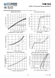
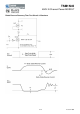
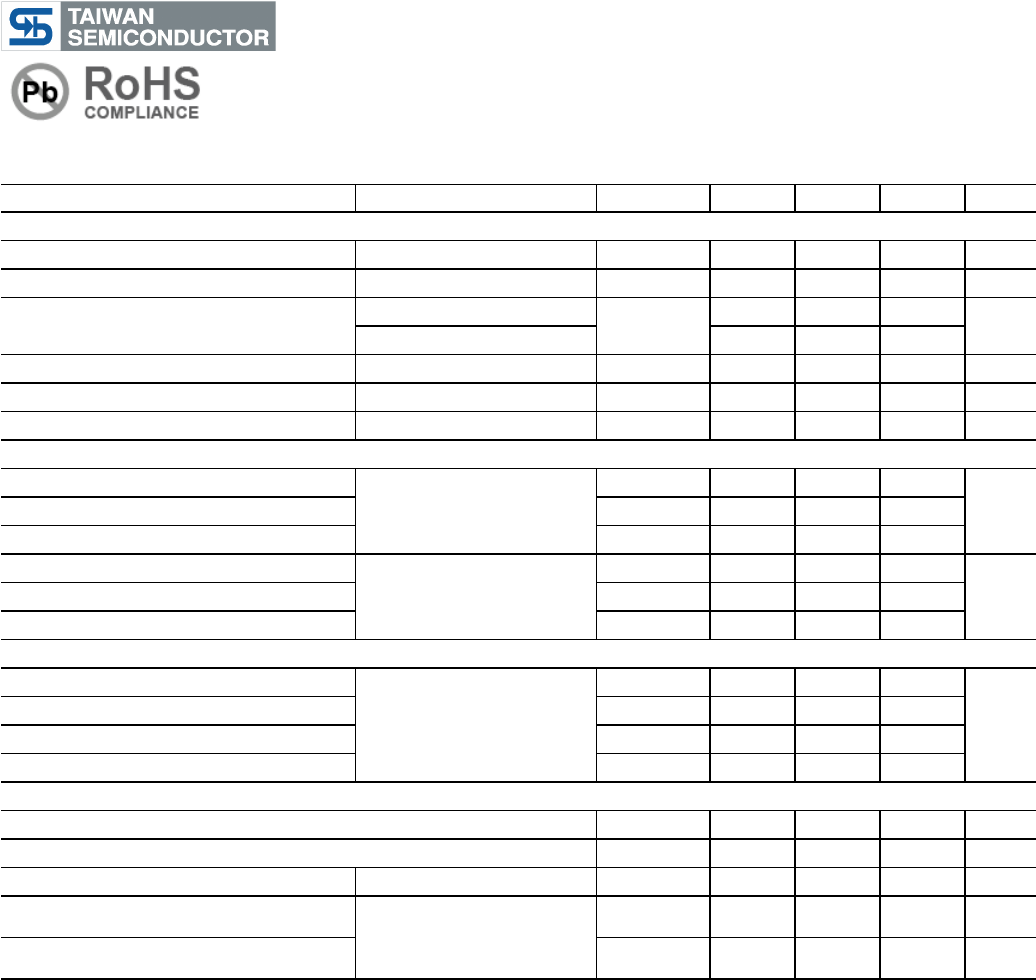
Electrical Specifications
(Ta=25
o
C, unless otherwise noted)
Parameter Conditions Symbol
Min Typ Max Unit
Static
Drain-Source Breakdown Voltage V
GS
= 0V, I
D
= 250uA BV
DSS
450 -- -- V
Drain-Source On-State Resistance V
GS
= 10V, I
D
= 0.25A R
DS(ON)
-- 3.7 4.25 Ω
Gate Threshold Voltage
V
DS
= V
GS
, I
D
= 250uA
V
GS(TH)
2.3 3.0 3.7
V
V
DS
= V
GS
, I
D
= 250mA 3.2 4.0 4.8
Zero Gate Voltage Drain Current V
DS
= 450V, V
GS
= 0V I
DSS
-- -- 10 uA
Gate Body Leakage V
GS
= ±30V, V
DS
= 0V I
GSS
-- -- ±100 nA
Forward Transconductance V
DS
= 50V, I
D
= 0.25A g
fs
-- 0.7 -- S
Dynamic
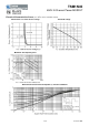
Total Gate Charge
V
DS
= 360V, I
D
= 0.5A,
V
GS
= 10V
(Note 4,5)
Q
g
-- 6.5 10
nC
Gate-Source Charge Q
gs
-- 1.3 --
Gate-Drain Charge Q
gd
-- 3.2 --
Input Capacitance
V
DS
= 25V, V
GS
= 0V,
f = 1.0MHz
C
iss
-- 235 --
pF
Output Capacitance C
oss
-- 29 --
Reverse Transfer Capacitance C
rss
-- 6.5 --
Switching
Turn-On Delay Time
V
GS
= 25V, I
D
= 0.5A,
V
DS
= 225V, R
G
= 25Ω
(Note 4,5)
t
d(on)
-- 14.7 --
nS
Turn-On Rise Time t
r
-- 32.8 --
Turn-Off Delay Time t
d(off)
-- 25.2 --
Turn-Off Fall Time t
f
-- 23.7 --
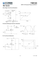
Drain-Source Diode Characteristics and Maximum Ratings
Maximum Continuous Drain-Source Diode Forward Current I
S
-- -- 0.5 A
Maximum Pulsed Drain-Source Diode Forward Current I
S
M
-- -- 4.0 A
Drain-Source Diode Forward Voltage
V
GS
= 0V, I
S
= 0.5A V
SD
-- -- 1.4 V
Reverse Recovery Time
V
GS
= 0V, I
S
= 1A
dI
F
/dt = 100A/µS
(Note 4)
t
rr
-- 110 -- nS
Reverse Recovery Charge Q
rr
-- 0.35 -- µC
Notes:
1. Repetitive Rating: Pulse width limited by maximum junction temperature
2. L=75mH, I
AS
=1.6A, V
DD
=50V, R
G
=25Ω, Starting T
J
=25ºC
3. I
SD
≤ 0.5A, di/dt ≤ 300A/µS, V
DD
≤ BV
DSS
, Starting T
J
=25ºC
4. Pulse test: pulse width ≤ 300uS.
5. Essentially independent of operating temperature
6. a) Reference point of the is the drain RӨ
JL
lead
b) When mounted on 3”x4.5” FR-4 PCB without any pad copper in a still air environment
(RӨ
JA
is the sum of the junction-to-case and case-to-ambient thermal resistance. RӨ
CA
is determined by the
user’s board design)