
Instruction Manual

TSM160N10
100V N-Channel Power MOSFET
2/6
Version: B13
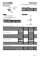
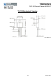
Electrical Specifications
(Ta = 25
o
C unless otherwise noted)
Parameter Conditions Symbol
Min Typ Max
Unit
Static
Drain-Source Breakdown Voltage V
GS
= 0V, I
D
= 250uA BV
DSS
100 -- -- V
Drain-Source On-State Resistance V
GS
= 10V, I
D
= 30A R
DS(ON)
-- 4.5 5.5 mΩ
Gate Threshold Voltage V
DS
= V
GS
, I
D
= 250uA V
GS(TH)
2 3 4 V
Zero Gate Voltage Drain Current V
DS
= 80V, V
GS
= 0V I
DSS
-- -- 1 uA
Gate Body Leakage V
GS
= ±20V, V
DS
= 0V I
GSS
-- -- ±100
nA
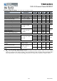
Dynamic
Total Gate Charge
V
DS
= 30V, I
D
= 30A,
V
GS
= 10V
Q
g
-- 154 --
nC
Gate-Source Charge Q
gs
-- 35 --
Gate-Drain Charge Q
gd
-- 40 --
Input Capacitance
V
DS
= 30V, V
GS
= 0V,
f = 1.0MHz
C
iss
-- 8600 --
pF
Output Capacitance C
oss
-- 780 --
Reverse Transfer Capacitance C
rss
-- 300 --
Switching
Turn-On Delay Time
V
GS
= 10V, V
DS
= 30V,
R
G
= 3.3Ω
t
d(on)
-- 25 --
nS
Turn-On Rise Time t
r
-- 40 --
Turn-Off Delay Time t
d(off)
-- 85 --
Turn-Off Fall Time t
f
-- 45 --
Drain-Source Diode Characteristics and Maximum Rating
Drain-Source Diode Forward
Voltage
V
GS
=0V, I
S
=30A V
SD
-- 0.8 1.3 V
Reverse Recovery Time
I
S
= 30A, T
J
=25
o
C
dI/dt = 100A/us
t
fr
-- 120 -- nS
Reverse Recovery Charge Q
fr
-- 160 -- nC
Notes:
1. Pulse Test: Pulse Width ≤ 300µs, Duty Cycle ≤ 2%.
2. Rθ
JA
is the sum of the junction-to-case and case-to-ambient thermal resistance where the case thermal
reference is defined as the solder mounting surface of the drain pins. Rθ
JC
is guaranteed by design while Rθ
CA
is determined by the user's board design. Rθ
JA
shown below for single device operation on FR-4 in still air