
User Manual
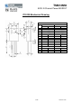

TSM13N50
500V N-Channel Power MOSFET
2/10
Version: C12
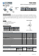
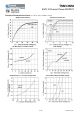
Electrical Specifications
(Ta = 25
o
C unless otherwise noted)
Parameter Conditions Symbol
Min Typ Max Unit
Static
Drain-Source Breakdown Voltage V
GS
= 0V, I
D
= 250uA BV
DSS
500 -- -- V
Drain-Source On-State Resistance V
GS
= 10V, I
D
= 6.5A R
DS(ON)
-- 0.38 0.48 Ω
Gate Threshold Voltage V
DS
= V
GS
, I
D
= 250uA V
GS(TH)
2.0 -- 4.0 V
Zero Gate Voltage Drain Current V
DS
= 500V, V
GS
= 0V I
DSS
-- -- 1 uA
Gate Body Leakage V
GS
= ±30V, V
DS
= 0V I
GSS
-- -- ±100 nA
Forward Transconductance V
DS
= 30V, I
D
= 6.5A g
fs
-- 14 -- S
Diode Forward Voltage I
S
= 13A, V
GS
= 0V V
SD
-- -- 1.5 V
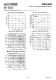
Dynamic
Total Gate Charge
V
DS
= 400V, I
D
= 13A,
V
GS
= 10V
Q
g
-- 36 --
nC
Gate-Source Charge Q
gs
-- 8.5 --
Gate-Drain Charge Q
gd
-- 8.7 --
Input Capacitance
V
DS
= 25V, V
GS
= 0V,
f = 1.0MHz
C
iss
-- 1918 --
pF
Output Capacitance C
oss
-- 187 --
Reverse Transfer Capacitance C
rss
-- 7.7 --
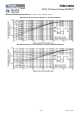
Switching
Turn-On Delay Time
V
DD
= 250V, I
D
= 13A,
R
G
= 25Ω
t
d(on)
-- 53 --
nS
Turn-On Rise Time t
r
-- 45 --
Turn-Off Delay Time t
d(off)
-- 156 --
Turn-Off Fall Time t
f
-- 59 --
Reverse Recovery Time
V
GS
= 0V, I
S
= 13A,
dI
F
/dt = 100A/us
t
fr
-- 325 -- nS
Reverse Recovery Charge Q
fr
-- 3.3 -- uC
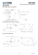
Notes:
1. Repetitive Rating: Pulse Width Limited by Maximum Junction Temperature
2. V
DD
= 50V, I
AS
=13A, L=6mH, R
G
=25Ω, Starting T
J
=25℃
3. I
SD
≤13A, di/dt ≤ 200A/uS, Vdd ≤ BV
DS
, Starting T
J
=25℃
4. Pulse test: pulse width ≤300uS, duty cycle ≤2%
5. b For design reference only, not subject to production testing.
6. c Switching time is essentially independent of operating temperature.