
Owner manual

TSM12N65
650V N-Channel Power MOSFET
2/8
Version: A10
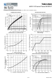
Electrical Specifications
(Ta = 25
o
C unless otherwise noted)
Parameter Conditions Symbol
Min Typ Max Unit
Static
Drain-Source Breakdown Voltage V
GS
= 0V, I
D
= 250uA BV
DSS
650 -- -- V
Drain-Source On-State Resistance V
GS
= 10V, I
D
= 6A R
DS(ON)
-- 0.68 0.8 Ω
Gate Threshold Voltage V
DS
= V
GS
, I
D
= 250uA V
GS(TH)
2.0 -- 4.0 V
Zero Gate Voltage Drain Current V
DS
= 650V, V
GS
= 0V I
DSS
-- -- 1 uA
Gate Body Leakage V
GS
= ±30V, V
DS
= 0V I
GSS
-- -- ±100 nA
Forward Transfer Conductance V
DS
= 10V, I
D
= 6A g
fs
-- 10 -- S
Dynamic
b
Total Gate Charge
V
DS
= 480V, I
D
= 12A,
V
GS
= 10V
Q
g
-- 41 --
nC
Gate-Source Charge Q
gs
-- 13 --
Gate-Drain Charge Q
gd
-- 10.5 --
Input Capacitance
V
DS
= 25V, V
GS
= 0V,
f = 1.0MHz
C
iss
-- 2162 --
pF
Output Capacitance C
oss
-- 183 --
Reverse Transfer Capacitance C
rss
-- 14.6 --
Switching
c
Turn-On Delay Time
V
GS
= 10V, I
D
= 12A,
V
DD
= 300V, R
G
=25Ω
t
d(on)
-- 30 --
nS
Turn-On Rise Time t
r
-- 85 --
Turn-Off Delay Time t
d(off)
-- 140 --
Turn-Off Fall Time t
f
-- 90 --
Source-Drain Diode Ratings and Characteristic
Source Current Integral reverse diode in
the MOSFET
I
S
-- -- 12 A
Source Current (Pulse) I
SM
-- -- 48 A
Diode Forward Voltage I
S
= 12A, V
GS
= 0V V
SD
-- -- 1.4 V
Reverse Recovery Time
V
GS
= 0V, I
S
=12A,
dI
F
/dt = 100A/us
t
fr
-- 510 -- nS
Reverse Recovery Charge Q
fr
-- 4.3 -- uC
Note 1: Repetitive Rating: Pulse Width Limited by Maximum Junction Temperature
Note 2: V
DD
= 50V, I
AS
=12A, L=3.5mH, R
G
=25Ω, Starting T
J
=25ºC
Note 3: Pulse test: pulse width ≤300uS, duty cycle ≤2%
Note 4: Essentially Independent of Operating Temperature