
User guide


TSM10N06
60V N-Channel MOSFET
2/6
Version: A10
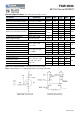
Electrical Specifications
(Ta = 25
o
C unless otherwise noted)
Parameter Conditions Symbol
Min Typ Max Unit
Static
Drain-Source Breakdown Voltage V
GS
= 0V, I
D
= 250uA BV
DSS
60 -- -- V
Gate Threshold Voltage V
DS
= V
GS
, I
D
= 250µA V
GS(TH)
1 -- 3 V
Gate Body Leakage V
GS
= ±20V, V
DS
= 0V I
GSS
-- -- ±100 nA
Zero Gate Voltage Drain Current V
DS
= 60V, V
GS
= 0V I
DSS
-- -- 2 µA
Drain-Source On-State Resistance
V
GS
= 10V, I
D
= 10A
R
DS(ON)
-- -- 65
mΩ V
GS
= 5V, I
D
= 10A -- -- 80
V
GS
= 4V, I
D
= 9A -- -- 110
Forward Transconductance V
DS
= 25V, I
D
= 6A g
fs
-- 13 -- S
Diode Forward Voltage I
S
= 2A, V
GS
= 0V V
SD
-- 0.9 1.2 V
Dynamic
2
Total Gate Charge
V
DS
= 30V, I
D
= 9A,
V
GS
= 4.5V
Q
g
-- 10.5 16
nC
Gate-Source Charge Q
gs
-- 3.5 --
Gate-Drain Charge Q
gd
-- 4.2 --
Input Capacitance
V
DS
= 30V, V
GS
= 0V,
f = 1.0MHz
C
iss
-- 1100 --
pF
Output Capacitance C
oss
-- 90 --
Reverse Transfer Capacitance C
rss
-- 55 --
Switching
2,3
Turn-On Delay Time
V
DD
= 30V, R
L
= 5.4Ω,
I
D
= 9A, V
GEN
= 10V,
R
G
= 1Ω
t
d(on)
-- 10 15
nS
Turn-On Rise Time t
r
-- 15 25
Turn-Off Delay Time t
d(off)
-- 25 40
Turn-Off Fall Time t
f
-- 10 15
Notes 1: Pulse test: PW
≤
300µS, duty cycle
≤
2%
Notes 2: For DESIGN AID ONLY, not subject to production testing.
Notes 3: Switching time is essentially independent of operating temperature.