
User guide

8
TS81102G0
2105C–BDC–11/03
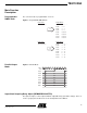
Single-ended
Output Data
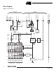
To reduce the pin number and power consumption of the DMUX, the eight output ports are
single-ended.
To reach the high frequency output (up to 250 MHz) with a reasonable power consumption,
the swing must be limited to a maximum of ±500 mV. The common mode is adjustable from
-1.3V to +2V, with Vplus DOut pins. To ensure better noise immunity, a reference level (com-
mon mode) is available (one level by output port).
The output buffers are of ECL type (open emitters – not resistive adapted impedances). They
are designed for a 15 mA average output current, and may be used with a 50Ω termination
impedance.
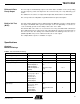
Figure 9. Single-ended Output Data
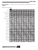
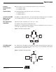
Following are three application examples for these buffers: ECL/PECL/TTL. Please note that it
is possible to have any other odd output format as far as current (36 mA max) and voltage
(Vplus Dout – V
EE
≤ 8.3V) limits are not overridden. The maximum frequency in TTL output
mode depends on the load to be driven.
This corresponds to the “Adjustable Logic Single” in the pinout description.
The “Adjustable Single” buffers for reference voltage are the same buffers, but the information
available at the output of these buffers is more like analog than logic.
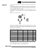
Note: The Max Output Data Rate is given for a typical 50Ω/2 pF load.
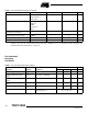
Table 1. Examples of Application of Buffers
Parameter ECL PECL TTL Unit
VplusDout 0 3.3 3.3 V
Vtt -2 1.3 0 V
Swing ±0.5 ±0.5 ±1 V
Reference -1.3 2 1.5 V
Voh -0.8 2.5 2.5 V
Vol -1.8 1.5 0.5 V
Load 50 50 ≥75 Ω
Average Output Current 14 14 15 mA
Output Data rate max. 250 250 250 Msps
Vee
PadOut
VPlusDOut