
User guide

14
TS81102G0
2105C–BDC–11/03
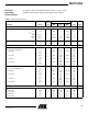
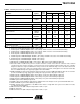
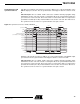
Synchronous Reset
Setup time from SyncReset to Clkln
DR input clock
DR/2 input clock
TSSR – –
–
-580
-477
–
–
ps
ps
(3)
(4)
Hold time from Clkln to SyncReset
DR input clock
DR/2 input clock
THSR – –
–
780
677
–
–
ps
ps
(5)
(6)
Rise/fall for (10% – 90%) TSRR/TFSR – 100 – – ps
Input Data
Setup time from I[0…9] to Clkln
DR input clock
DR/2 input clock
TSCKIN – –
–
-794
-691
–
–
ps
ps
(7)
(8)
Hold time from Clkln to I[0…9]
DR input clock
DR/2 input clock
THCKIN – –
–
994
891
–
–
ps
ps
(9)
(10)
Rise/fall for (10% – 90%) TRDI/TFDI – 100 – – ps
Output Data
Data output delay
DR input clock
DR/2 input clock
TOD – –
–
1820
1717
–
–
ps
ps
(11)
(12)
Data pipeline delay
DR input clock, 1:4 ratio
DR input clock, 1:8 ratio
DR/2 input clock, 1:4 ratio
DR/2 input clock, 1:8 ratio
TPD –
–
–
–
–
3
7
3/2
7/2
–
–
–
–
Number
of input
clock
(13)
Rise/fall for (10% – 90%) TROD/tfod – – 497/484 – ps
(14)
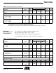
Data Ready
Data ready Falling edge
DR input clock
DR/2 input clock
TDRF – –
–
1856
1753
–
–
ps
ps
(15)
(16)
Data ready Rising edge
DR input clock
DR/2 input clock
TDRR – –
–
1828
1725
–
–
ps
ps
(17)
(18)
Asynchr; Reset to DataReady delay TARDR – – 1918 – ps
(19)
Synchr. Reset to DataReady delay TSRDR – – 1037 – ps
(20)
Rise/fall for (10% – 90%) TRDR/TFDR – – 450 – ps
(21)
Rising edge uncertainty JITTER – – 62 – ps
Built-In Self Test
Hold time from Clkln to BIST THBIST – – – – ps
(22)
Table 5. Switching Performances (Continued)
Parameter Symbol
Test
Level
Value
Unit NoteMin Typ Max