
User guide

13
TS81102G0
2105C–BDC–11/03
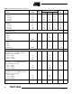
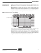
Note: 1. The supply current I
PLUSD
and the power dissipation depend on the state of the output buffers:
- the minimum values correspond to all the output buffers at low level,
- the maximum values correspond to all the output buffers at high level,
- the typical values correspond to an equal sharing-out of the output buffers between high and low levels.
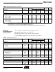
Switching
Performance and
Characteristics
50% clock duty cycle (CLKIN, CLKINB). Tj (typical) = 70°C.
Full temperature range: -40°C < Tc; Tj < 110°C.
(Guaranteed temperature ranges depend on the part number)
See Timing Diagrams Figure 10 on page 16 to Figure 19 on page 21.
Output level drift with temperature (reference
outputs)
–1–-0.9–mV/
°C
Digital Inputs
ECL Input Voltages
Logic “0” voltage
Logic “1” voltage
V
IL
V
IH
1
–
-1.1
–
–
-1.4
–
V
V
TTL Input Voltages
Logic “0” voltage
Logic “1” voltage
V
IL
V
IH
1
–
2.0
–
–
0.8
–
V
V
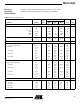
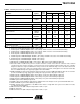
Table 4. Electrical Specifications (Continued)
Parameter Symbol
Test
Level
Value
Unit NoteMin Typ Max
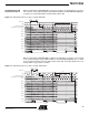
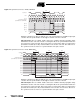
Table 5. Switching Performances
Parameter Symbol
Test
Level
Value
Unit NoteMin Typ Max
Input Clock
Maximum clock frequency
1:8 ratio
1:4 ratio
FMAX – 2
1
–
–
2.2
1.1
GHz
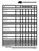
Clock pulse width (high) TC1 – 100 – – ps
Clock pulse width (low) TC2 – 100 – – ps
Clock Path pipeline delay
DR input clock
DR/2 input clock
TCPD
TCPD
––
–
981
1084
–
–
ps
ps
(1)
(2)
Clock rise/fall time TRCKIN
TFCKIN
– – 100 – ps
Asynchronous Reset
Asynchronous Reset pulse width PWAR – 1000 – – ps
Setup time from Asynchronous to Clkln TSAR – – 1500 – ps
Rise/fall time for (10% – 90%) TRAR
TFAR
– 1000 – – ps