
Manual
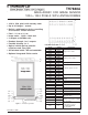

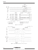

EXPOSURE TIME REDUCTION
TH7888A allows exposure time control (electronic shutter function).
The exposure time reduction is achieved by pulsing all the FPi gates to 0 volt so as to remove continuously all the photoge-
nerated electrons through antiblooming drain VA.
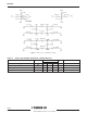
Figure 10 : Timing diagram for electronic shutter
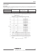
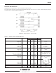
TABLE 2 - DRIVE CLOCK CHARACTERISTICS
Parameter Symbol Value Unit Remarks
Min Typ Max
Image zone clocks FP1,2, 3,4
Typical input capacitance
15 nF
See figure 11
High level 7.5 8 8.5 V
Low level 0 0.5 0.8 V
Memory zone clocks FM1,2,3,4
Typical input capacitance
15.5 nF
See figure 11
High level 7.5 8 8.5 V
Low level 0 0.5 0.8 V
Memory to register clocks FM
Typical input capacitance
10 pF
High level 8.5 9 9.5 V
Low level 0 0.5 0.8 V
Antiblooming gate FA
Typical input capacitance
14 nF
See figures 11 & 13
High level (integration) 3 4 7 V
Low level (transfer) 0 0.5 0.8 V
Reset gate FR
Typical input capacitance
10 pF
High level 10 12 13 V
Low level 0 2 3 V
Readout register clocks FL1,2
High level 8.5 9 9.5 V
Low level 0 0.5 0.8 V
Maximum readout register frequency F
H
20 23 MHz See figure 7
Image zone to memory zone transfer
frequency
F
V
1.25 1.7 MHz See figure 12
9/16
TH7888A
Fall times & rise times : see fig.5&6