
User Manual

5
TH7841A
1998A–IMAGE–05/02
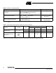
Notes: 1. V
OS
= average video output voltage. Measurement excludes first and last pixels.
2. F
S
=2FΦ
T
. The minimum clock frequency is limited by the increase in dark signal.
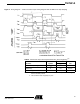
Electro-optical
Performance
General measurement conditions: T
C
=25°C; T
i
=1ms;FΦ
T
=2.5MHz.
Light source: tungsten filament lamp (2854 K) + BG 38 filter (2 mm thick) + F/3.5 aper-
ture. The filter limits the spectrum to 700 nm; in these conditions, 1 µJ/cm
2
corresponds
to 3.5 lux.s.
Typical operating conditions; internal clock mode (see Table 2).
First and last pixels, as well as reference elements, are excluded from the specification.
Measurements taken on each output in succession.
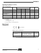
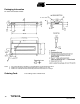
Table 4. Static and Dynamic Electrical Characteristics
Parameter Symbol
Values
Unit NoteMin Typ Max
DC Output Level V
REF
81012V
Output Impedance Z
S
500 Ω
Register Single-stage Transfer Efficiency CTE 99.992 99.998 % V
OS
=1V
(1)
Max. Data Output Frequency F
S
max. 12 20 MHz
(2)
Input Current on Pins: 3, 5, 10,11,12, 13,
18, 19, 20, 21, 25
Ie 2 µA
Ve = 15V
All other pins: 0V
Peak Current Sink on Φ
T
Clock (IΦ
T
)
P
500 mA t
rise
=15ns
Peak Current Sink on Φ
P
Clock (IΦ
P
)
P
125 mA t
rise
=15ns
Output Amplifier Drain Supply Current I
DD
17 mA
V
INH
=0V
V
DD
=15V
Static Power Dissipation P
D
255 300 mW
V
INH
=0V
V
DD
=15V