
User Manual

4
TH7841A
1998A–IMAGE–05/02
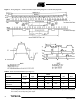
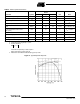
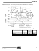
Figure 1. Timing Diagram — Clocks and Video Output Timing Diagram in Internal Sampling Mode
Note: 1. Transients under 0.0V in the clock pulses will lead to charge injection, causing a localized increase in the dark signal if such
spurious negative transients are present, they can be suppressed by inserting a serial resistor of appropriate value (typically
20 to 100Ω) in the corresponding driver output.
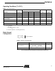
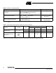
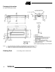
Table 3. Drive Clock Characteristics (see Figure 1)
Parameter Symbol Logic
Values
Unit NoteMin Typ Max
Transfer Clock
Φ
P
Φ
T
High 12 13 14 V
(1)
Register Transport Clock Low 0.0 0.4 0.6
Register Transport Clock
Capacitance
CΦ
T
800 1200 pF
Transfer Clock Capacitance CΦ
P
200 300 pF