
User guide


3
TH7813A/TH7814A
1990A–IMAGE–05/02
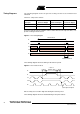
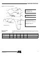
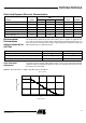
Figure 1. Readout Register Clocks Capacitance TH7813
Figure 2. Readout Register Clocks Capacitance TH7814
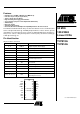
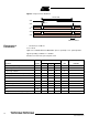
Register Output Gate Bias VGS 2.2 2.4 2.6 V
Output Amplifier Source Supply VS 0 V
Ground VSS 0
Table 2. Drive Clocks Characteristics
Parameter Symbol
Value
Unit RemarkMin. Typ. Max.
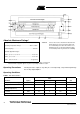
Reset gate
High level
Low level
ΦR
8.5
-0.1
9
0
9.5
0.4
V
V
Clock Capacitance < 25 pF
Transfer gate
High level
Low level
ΦP
8.5
-0.1
9
0
9.5
0.4 V
V
Clock Capacitance < 100 pF
Readout register clocks
Hilgh level
Low level
ΦL1, 2
8.5
-0.1
9
0
9.5
0.4 V
V
see Figure 1 and Figure 2
Maximum readout register
frequency
F
H
10 25 MHz
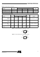
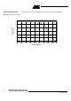
Table 1. DC Characteristics (Continued)
Parameter Symbol
Value
UnitMin Typ Max
50 pF
140 pF120 pF
ΦL1 ΦL2
100 pF
230 pF230 pF
ΦL1 ΦL2