
User Manual

97
T89C51AC2
Rev. B – 19-Dec-01
Figure 44. Cl ock Signal W ave form for I
CC
Tests i n A c ti v e and Idle Modes
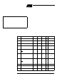
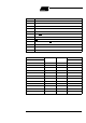
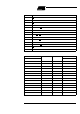
18.3 DC Parameters for A/D Converter
Table 58. DC P arameters for A D Convert er in Precision conv ers ion
Notes: 1. Typicals are based on a limited number of samples and are not guaranteed.
18.4 AC Parameters
18.4.1 Explanation of the AC
Symbols
Each timing symbol has 5 characters. The first character is alway s a “T” (stands for
time). The other charact ers , depending on their positions , stand for the nam e of a signa l
or the logical status of that signal. The following is a list of all the characters and what
they stand for.
Example:T
AVLL
= Time for Address Valid to ALE Low.
T
LLPL
= Tim e for ALE Low to PSEN Low.
T
A =-40°Cto+85°C; V
SS
=0V;V
CC
=5V±10%; F = 0 to 40 MHz.
T
A =-40°Cto+85°C; V
SS
=0V;V
CC
=5V± 10%.
( Load Cap acita nc e for port 0, ALE and PSE N = 60 pF; Load Capacitance for all other
outputs = 60 pF.)
Table 59, Table 62 and T able 65 give the description of each AC symbols.
Table 60, Table 63 and Table 66 give for each range the AC param et er.
Table 61, Table 64 and Table 67 give the frequency derating f ormul a of th e AC parame-
ter for each speed range description. To calculate each AC symbols. take the x value
and use this value in the formula.
Example: T
LLIV
and 20 MHz, Sta ndard clock.
x = 30 ns
T = 50 ns
T
CCIV
= 4T - x = 170 ns
V
CC
-0.5V
0.45V
0.7V
CC
0.2V
CC
-0.1
T
CLCH
T
CHCL
T
CLCH
=T
CHCL
=5ns.
Symbol Parameter Min Typ
(1)
Max Unit Test Conditions
AVin Analog input voltage Vss- 0.2
Vref +
0.2
V
Rref Resistance between Vref and Vss 12 16 24
KO
hm
Vref Reference voltage 2.40 3.00 V
Cai Analog input Capacitance 60 pF During sampling
INL Integral non linearity 1 2 lsb
DNL Differential non linearity 0.5 1 lsb
OE Offset error -2 2 lsb