
User Manual

94
T89C51AC2
Rev. B – 19-Dec-01
18. Electrical Characteristics
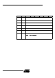
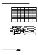
18.1 Absolute Maximum
Ratings
(1)
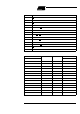
18.2 DC Parameters for Standard Voltage
TA =-40°Cto+85°C; V
SS
=0V;V
CC
=5V± 10%; F = 0 to 40 MHz.
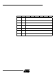
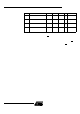
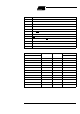
Table 57. DC P arameters in Sta ndard Voltage
Am biant Temperat ure Under Bias:
I = industrial.................................................-40°Cto85°C
Storage Temperature ............................-65°C to + 150°C
Voltage on V
CC
from V
SS..........................................
-0.5 V to + 6V
Voltage on A ny Pin f r om V
SS
............-0.5 V to V
CC
+0.2V
Power Dissipation................................................... 1 W
(2)
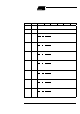
Symbol Parameter Min Typ
(5)
Max Unit Test Conditions
V
IL
Input Low Voltage -0.5
0.2Vcc -
0.1
V
V
IH
Input High Voltage except XTAL1,
RST
0.2 V
CC
+
0.9
V
CC
+0.5 V
V
IH1
Input High Voltage, XT AL1, RST 0.7 V
CC
V
CC
+0.5 V
V
OL
Output Low Voltage, ports 1, 2, 3
and 4
(6)
0.3
0.45
1.0
V
V
V
I
OL
= 100 µA
(4)
I
OL
=1.6mA
(4)
I
OL
=3.5mA
(4)
V
OL1
Output Low Voltage, port 0, ALE,
PSEN
(6)
0.3
0.45
1.0
V
V
V
I
OL
= 200 µA
(4)
I
OL
=3.2mA
(4)
I
OL
=7.0mA
(4)
V
OH
Output High Voltage, ports 1, 2, 3,
4and5
V
CC
-0.3
V
CC
-0.7
V
CC
-1.5
V
V
V
I
OH
=-10µA
I
OH
=-30µA
I
OH
=-60µA
V
CC
=5V± 10%
V
OH1
Output High Voltage, port 0, ALE,
PSEN
V
CC
-0.3
V
CC
-0.7
V
CC
-1.5
V
V
V
I
OH
=-200µA
I
OH
=-3.2mA
I
OH
=-7.0mA
V
CC
=5V± 10%
R
RST
RST Pulldown Resistor 20 40 200 kΩ
I
IL
Logical 0 Input Current ports 1, 2,
3and4
-50 µAVin=0.45V
I
LI
Input Leakage Current ±10 µA
0.45 V < Vin <
V
CC
Note: Stresses at or above those listed under “Absolute Maximum
Ratings” may cause per manent damage to the device. This
is a stress r ating only and functional operation of the device
at these or any other conditions above those indicated i n
the operational sections of this specification is not implied.
Exposure to absol ute maximum rating conditions may aff ect
device reliability.This value is based on the maximum allow-
able die temperature and the thermal resistance of the
package.