
User Manual

9
T89C51AC2
Rev. B – 19-Dec-01
It is not obv ious the l as t three instructions in th is l ist are Read-M odify-Write inst ru ctions.
These instructions read the port (all 8 bits), modif y the specifically addressed bit and
write the new byte back to th e latch. T hes e Read-M odify-W rite instruc tions are directed
to the latch rather than the pin in order to avoid possible misint erpretation of voltage
(and therefore, logic) levels at t he pi n. For exam ple, a Port bit used t o dri ve t he base of
an external bipolar transis tor can not rise above the transistor’s base-emitter junction
voltage (a value lower than VIL). With a lo gic one written to the bit, attempts by the CP U
to read the Port at the pin are misinterpreted as logic zero. A read of the latch rather
than the pins ret urns the correc t logic-one value.
4.5 Quasi-Bidirectional
Port Operation
Port 1, Port 2, P ort 3 a nd P ort 4 hav e fixed intern al pull-ups an d are ref erred to as
"qua si-b idirectional" Port s . W hen configured a s an input, the pin impedance appears as
logic on e and sources current in response to an external logic zero cond ition. P ort 0 i s a
"true bidirectional" pin. The pins float when configured as inpu t. Resets write logi c one to
all P ort latches. If logical z ero is subs equent ly written to a Port latch, it can be returned
to input con ditions by a logical o ne written to the latch.
Note: Port latch values change near t he end of Read-Modify- Write i nstruction cycles. Output
buffers (and t herefore t he pin stat e) update early in the instruction aft er Read-Modif y-
Write instruction cycle.
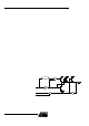
Logical zero-to-one transitions in Port 1 , Port 2, Port 3 and Port 4 use an additional pull-
up (p1) to aid this logic transition (see Figure 4. ). This increases switch s peed. T his
ex tra pull- up s ourc es 100 t imes normal internal circuit curre nt duri ng 2 o s c illat or cloc k
periods. The internal pull-ups are field-effect transistors rather than linear resistors. Pull-
ups con sis t of three p-channel FET (pFET) de vice s. A pFET is on when the gate senses
logical zero and of f w hen the gate s enses logical one. pFET #1 is turned on for two
oscillator periods immediately after a zero-to-one transition in the Port latch. A logical
one at the Port pin turns on pFET #3 (a weak pull-up) through the invert er. This inverter
and pFET pair form a latch to drive logical one. pFET #2 is a very w eak pull -u p sw itch ed
on whenever the associated nFE T is switche d off. This is traditional CMO S s witch con-
vention . Current strength s are 1/10 that of pFET #3.
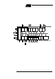
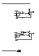
Figure 4. Internal Pull-Up Configurations
Note: Port 2 p1 assists the logic-one out put for memory bus cycles.
READ PIN
INPUT DATA
P1.x
OUTPUT DATA
2 Osc. PERIODS
n
p1(1)
p2
p3
VCCVCCVCC
P2.x
P3.x
P4.x