
User Manual

82
T89C51AC2
Rev. B – 19-Dec-01
16.3 ADC Converter
Operation
A start of single A /D conversion is triggered b y s et ting bi t A DSST (ADCON.3).
After c ompletion of t he A/D conversion, the ADSST bit is cleared by hardware.
The end-of - c onv ers ion f lag A D EO C (ADCON.4 ) is s et when the v alue of convers ion is
available in ADDH and ADDL, it must be cleared b y software. If the bit E A D C (IEN1.1) is
s et, an interrupt occur when flag A DEO C is set (see Fi gure 39). C lear th is fl ag for re-
arming the interrupt.
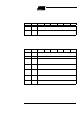
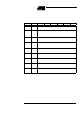
ThebitsSCH0toSCH2inADCONregisterareusedfortheanaloginputchannel
selection.
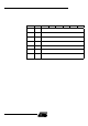
Table 43. Selected Analog input
16.4 Voltage Conversion When the ADCIN is equals to VAREF the ADC converts the signal to 3FFh (full sc ale). If
the input v oltage equals VAGND, the ADC converts it to 000h. Input v oltage between
VAREF and VA GND are a straight-line linear convers ion. All ot her voltages will result in
3FFh if greate r t han VAREF and 000h if less t han VAGND.
Note t hat ADCIN should not exceed VAREF absolute m aximum range! (see section
“AC-DC”)
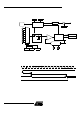
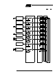
16.5 Clock Selection The ADC clock is the same as CPU.
The maximum clock frequen cy for ADC is 700KHz. A prescaler is featured (ADCCLK) to
generate the ADC clock from the oscillator frequency .
Figure 38. A/D Converter cloc k
SCH2 SCH1 SCH0 Selected Analog input
000AN0
001AN1
010AN2
011AN3
100AN4
101AN5
110AN6
111AN7
Prescaler ADCLK
A/D
Converter
ADC Clock
CPU
CLOCK
CPU Core Clock Symbol
÷ 2