
User Manual

81
T89C51AC2
Rev. B – 19-Dec-01
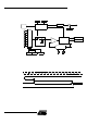
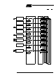
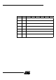
Figure 36. ADC Descripti on
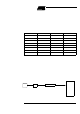
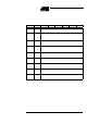
Figure 37 shows the timing diagra m of a com plete convers ion. F or simplicity, th e figure
depict s t he wave fo rms in ideali z ed form a nd do not prov ide prec ise timi ng inf ormation.
For ADC charac teristics a nd tim ing paramet ers refer to the Section “AC Characte ristics”
of the T89C51A C2 datasheet.
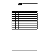
Figure 37. T im ing Diagram
Note: Tsetup min = 4 us
Tconv=11 clock ADC = 1sample and hold + 10 bit conversion
The user must ensure that 4 us minimum time between setti ng ADEN and the start of the
first convers ion.
AN0/P1.0
AN1/P1.1
AN2/P1.2
AN3/P1.3
AN4/P1.4
AN5/P1.5
AN6/P1.6
AN7/P1.7
000
001
010
011
100
101
110
111
SCH2
ADCON.2
SCH0
ADCON.0
SCH1
ADCON.1
ADC
CLOCK
ADEN
ADCON.5
ADSST
ADCON.3
ADEOC
ADCON.4
ADC
Inter rupt
Request
EADC
IEN1.1
CONTROL
AVSS
Sample and Hold
ADDH
VAREF
R/2R DAC
VAGND
8
10
+
-
ADDL
2
SAR
ADCIN
ADEN
ADSST
ADEOC
T
SETUP
T
CONV
CLK