
User Manual

8
T89C51AC2
Rev. B – 19-Dec-01
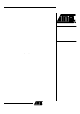
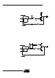
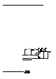
Figure 3. Port 2 Structure
Notes: 1. Port 2 is precl uded from use as general purpose I/O Ports w hen as address/data bus
driver s.
2. Port 2 internal strong pull-ups FET (P1 in FiGURE) assist the logic-one output for
memory bus cycle.
W hen Port 0 and Port 2 are u se d for an external memo ry cycle, an internal control signal
switches the out put -driver input from the latch output to the in ternal addres s/data line.
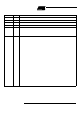
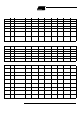
4.4 Read-Modify-Write
Instructions
Som e instructions read the latch data rat her than the pin data. T he latch ba se d i ns truc-
tions read the data, modify the data and then rewrite the latch . These are c alled "R ead-
Modify -Write" instructions. B elow is a complete list of these special instructions (see
Tabl e 2). Wh en the destination operand i s a Port or a Port bit, the s e inst ruc t ions read
the lat c h rather than t he pin:
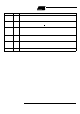
Table 2. Read-M odify-Write Instructions
D
Q
P2.X
LATCH
INTERNAL
WRITE
TO
LATCH
READ
PIN
READ
LATCH
0
1
P2.x (1)
ADDRESS HIGH/
CONTROL
BUS
VDD
INTERNAL
PULL-UP (2)
Instruction Description Example
ANL logical AND ANL P1, A
ORL logical OR ORL P2, A
XRL logical EX-OR XRL P3, A
JBC jump if bit = 1 and clear bit JBC P1.1, LABEL
CPL complement bit CPL P3.0
INC increment INC P2
DEC decrement DEC P2
DJNZ decrement and jump if not zero DJNZ P3, LABEL
MOV Px.y, C move carry bit to bit y of Port x MOV P1.5, C
CLR Px.y clear bit y of Port x CLR P2.4
SET Px.y set bit y of Port x SET P3.3