
User Manual


6
T89C51AC2
Rev. B – 19-Dec-01
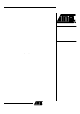
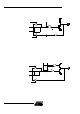
4.1 I/O Configurations Each Port SFR operates via type-D latches, as illustrated in Figure 1 for Port s 3 and 4. A
CPU "write to latch" signal initiates transfer of int ernal bus data into the type-D latch . A
CPU "read latch" signal transfers the latched Q output onto the internal bus. S im ilarly, a
"read pin " signal transfers the log ical level of the Port pin. Some Port data ins tructions
activate the "read latch" signal while ot hers activate the "read pin" signal. Latc h i ns truc-
tio ns are referre d to as R ead-M odif y-Write i nstructio ns. Ea ch I/O lin e may b e
independently programm ed as i nput or out put .
4.2 Port 1, Port 3 and
Port 4
Figure 1 shows the structure of Ports 1 and 3, wh ich ha ve internal pull -ups . An externa l
source can pull the pin low. E ach P ort pin can be configure d either for general purpos e
I/O or for its alternate input output function.
To use a pin for general purpos e output, set or clear the corresponding bit in the Px reg-
ister (x =1, 3 o r 4). To use a pin for ge neral p urpose input , set the bit in the P x regi s ter.
This turns off the output FET drive.
To configure a pin for its alternate function, set the bit i n the P x register. When the latch
is set, the "alternate output function" s ignal c ontrols t he output level (see Fig ure 1). T he
operation of Port s 1, 3 and 4 is discus se d furthe r in " quasi-Bidirectional Port Operation"
para graph.
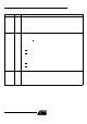
RESET I/O
Reset:
A high level on this pin during two machine cycles while the oscillator is running resets the device. An internal pull-
down resistor to VSS permits power-on reset using only an external capacitor to V CC.
ALE O
ALE:
An Address Latch Enable output for latching the low byte of the address during accesses to the external memory. The
ALE is activated every 1/6 oscillator periods (1/3 in X2 mode) except during an external data memory access. When
instructions are executed from an internal FLA SH (EA
= 1), ALE generation can be disabled by the software.
PSEN O
PSEN
:
The Program Store Enable output is a control signal that enables the external program memory of the bus during
external fetch operations. It is activated t wice each machine cycle during fetches from the external program memory.
However, when executing from of the external program memory two activations of PSEN are skipped during each
access to the external Data memory. The PSEN is not activated for internal fetches.
EA I
EA
:
When External Access is held at the high level, instructions are fetched from the internal FLASH when the program
counter is less t hen 8000H. When held at the low level,T89C51AC2 fetches all instructions from the external p rogram
memory
.
XTAL1 I
XTAL1:
Input of the inverting oscillator amplifier and input of the internal clock generator circuits.
To drive the device from an external clock source, XTAL1 should be driven, while XTAL2 is left unconnected. To
operate above a frequency of 16 MHz, a duty cycle of 50% should be maintained.
XTAL2 O
XTAL2:
Output from the inverting oscillator amplifier.
Pin Name Type Description