
User Manual


51
T89C51AC2
Rev. B – 19-Dec-01
12. Timers/Counters The T89C51AC2 implem ents two general-purpose, 16-bit Timers/Counters. Such are
ident ified as Timer 0 and Tim er 1, and can be independently configured to operate in a
va riety o f m odes as a T ime r or a n ev ent Co unte r. W he n op era ting as a T ime r, the
Timer/ Count er ru ns for a program med len gth of time , then iss ues an interrupt request.
W hen operating as a Counter, the Timer/C ounter c ounts negat ive trans itions on an
external pin. A fter a preset nu mber of counts, the Counter issues an interrupt request.
The v arious operat ing mod es of ea ch T imer/Coun ter are d escribed i n the f ollowing
sections.
12.1 Timer/Counter
Operations
A basic opera tion is Timer registers THx and TLx (x= 0, 1) co nnec ted in cas c ade to form
a 16-b it Timer. Set ting th e run cont rol bit (TRx) in TCON register (see Figure 20) turns
the Timer on by allowing the selected input to increment TLx. When TLx overflows it
increments THx; when THx ov erf lows it s ets the Timer overf low flag (TFx) in T CON reg-
ist er. Set t ing the TRx does not clea r the THx a nd TLx Tim er regist ers . T im er reg iste rs
can be accessed to obtain the current count or to enter preset values. They c an be read
at any time but TR x bit m us t be cleared to preset their values, otherwise the behavio r of
the Timer/Counter is unpredictable.
The C/Tx# control bi t selects Timer operation or Cou nter o peration by selecting the
div ided-down peripheral clock or external pin Tx as the source for the counted signal.
TRx bit must be cleared when changing th e mode of operation, otherwise the behavior
of the Time r/Counter is unpredictable.
For Timer op erat ion (C/Tx #= 0), t he Timer register c ounts th e divided-down peripheral
clock. T he Time r register is inc r emented on ce every peripheral cycle (6 peripheral clock
periods). The Timer clock rate is F
PER
/6,i.e.F
OSC
/ 12 in standard mode or F
OSC
/6in
X2 mode.
For Counter operation (C/T x #= 1), the Ti mer register counts the negative t ra ns itions on
the Tx external input pi n. T he external input is sampl ed e very peripheral cycles. When
the sample is high in one cycle and low in the next one, the Counter is incremented.
Since it takes 2 cycles (12 peripheral clock periods) to recognize a negative tra nsition,
the maximum count rate is F
PER
/ 12, i.e. F
OSC
/ 24 in standard mode or F
OSC
/12inX2
mode. There are no restrictions on the duty cycle of the ex ternal input signal, but to
ensure that a given level is s ampled at least once before it c hanges , it should be held for
at least one f ull peripheral c ycle .
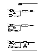
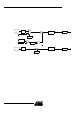
12.2 Timer 0 Timer 0 functions as either a Timer or event Counter in four modes of operation.
Figure 22 to Figure 25 show the logical configuration o f each mode.
Timer 0 is cont rolle d by the four lower bits of TMO D register (s ee Figure 2 1) and bits 0,
1, 4 and 5 of TCON regi ster (see Figure 20). TMO D register selects t he method of Timer
gat ing (GA TE0), Timer or Counter operat ion (T/C0#) and mode of operat ion (M10 and
M00). TCON register provid es Timer 0 control functions: overflow flag (TF0), run control
bit (TR0), i nte rrupt flag (IE0) and i nterrup t type control bit (IT0).
For no r mal Timer op erat ion (GAT E0= 0), s etting TR0 all ows T L0 to be i nc r emented by
the s elect ed input . Setting GA TE 0 and TR 0 a ll ows exte rnal pin INT 0# to c ontrol Timer
operation.
Timer 0 overf low (count rolls over from all 1s to all 0s ) sets TF0 flag generating an inter-
rupt request.
It is important to st op Timer/Count er bef ore changing mode.
12.2.1 M ode 0 (13-bit Timer) Mode 0 c onfigures Timer 0 as an 13-bit Timer which is set up as an 8-bit Timer (TH0
register) with a m odulo 32 presca ler implement ed with the lower five bits of TL0 register
( s ee Figure 22). The upper three bits o f T L0 regist er are i ndet ermin at e and should b e
ignored. P res c aler overflow increments TH0 regist er.