
User Manual


33
T89C51AC2
Rev. B – 19-Dec-01
9.3 Overview of FM0
operations
The CPU interfaces to the flash memory through the FCON register and A UXR1
register.
These registers are used to:
• Map the memory spaces in the adres sable spac e
• Launc h the programming of the memory spaces
• Get t he status of t he flash m emory (busy /not busy)
9.3.1 Mapping of the memory
space
By default, the user space is acces se d by MOVC instruc tion for read only. The column
latches space is m ade ac cessible by s etting the FPS bit in FCON re gister. W riting is
possi ble from 0000h to 7FFFh, address bit s 6 to 0 are used t o select an addres s w ithin a
page while bits 14 to 7 are used to sele ct the programming address of th e page.
Setting FPS bi t takes precedence on the EXTRAM bit in AUXR register.
The oth er mem ory spaces (user, extra row, hardware se c urity ) are m ade accessible i n
the c ode segment by programming bits FMOD0 and FMO D1 in FCON register in accor-
dance with Table 9. A MOVC instruction is then used for reading these spaces.
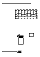
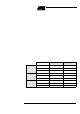
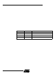
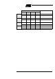
Table 9. .FM0 blocks select bits
9.3.2 Launching programming FP L3:0 bits in FCON register are used to secure the launch of pro gramm ing. A specif ic
se quenc e must be written in these bits to unlock the writ e protection and to launch th e
programm ing. This seq uenc e i s 5xh follo wed by Axh. Table 10 summarizes the m emory
spaces to program acc ording to FMO D1:0 bits.
FMOD1 FMOD0 FM0 Adressable space
0 0 User (0000h-FFFFh)
0 1 Extra Row(FF80h-FFFFh)
1 0 Hardware Security Byte (0000h)
11reserved