
User Manual


31
T89C51AC2
Rev. B – 19-Dec-01
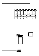
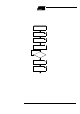
Figure 10. Ex ternal Code Fetch Waveforms
9.2 FLASH Memory
Architecture
T89C51A C2 featur es t w o on-chip flash memories:
• Flash memory FM0:
containing 32 Kby tes of program m emory (user space) organized into 128 byte
pages,
• Flash memory FM1:
2 Kbyt es f or boot loader and Appl icat ion Programming Interfaces (API ).
The FM0 can be program by both parallel program ming and Serial In-System P r ogram-
ming (ISP) whereas FM 1 supports only parallel programming by programmers. The ISP
mode is det ailed in the "In-System Programm ing" section.
All Read/Wri te access operations on F LASH Memory by user application are managed
by a set of API des c r ibed in the "I n-Syst em Programming" sec t ion.
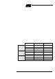
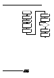
Figure 11. Flash memory arc hitecture
ALE
P0
P2
PSEN#
PCL
PCHPCH
PCLD7:0 D7:0
PCH
D7:0
CPU Clock
7FFFh
32 Kbytes
Flash memory
FM0
0000h
Hardware Security (1 byte)
Column Latches (128 bytes)
user space
Extra Row (128 bytes)
2Kbytes
Flash memory
FM1
boot space
FFFFh
F800h
FM1 mapped between FFFFh and
F800h when bit ENBOOT is set in
AUXR1 register