
User Manual


30
T89C51AC2
Rev. B – 19-Dec-01
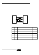
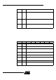
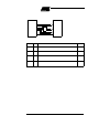
Figure 9. External Code Mem ory Int erface Structure
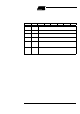
Table 7. Ex ternal Code Memo ry Interface Signals
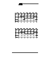
9.1.2 External Bus Cyc les This s ection d escribes the bus cycles the T8 9C51AC2 ex ecutes to fe tch c ode (see
Figure 10) in the external program/cod e m emory.
External m emory cycle takes 6 C PU clock periods. This is equivalent to 12 oscillator
clock period in s tandard mode o r 6 oscillator clock pe riods in X2 mode. For further infor-
mation on X 2 m ode see section “Clock “.
For simplicity, the a ccomp anying figu re de picts the bus cycle w aveforms in idealized
form and do not provide precise timing information.
For bus cyc ling parameters ref er to the section "AC-DC parameters".
FLASH
EPROM
T89C51AC2
P2
P0
AD7:0
A15:8
A7:0
A15:8
D7:0
A7:0
ALE
Latch
OEPSEN#
Signal
Name Type Description
Alternate
Function
A15:8 O
Address Lines
Upper address lines for the external bus.
P2.7:0
AD7:0 I/O
Address /Data Lines
Multiplexed lower address lines and data for the external memory.
P0.7:0
ALE O
Address Latch Enable
ALE signals indicates that valid address information are available on lines
AD7:0.
-
PSEN# O
Program Store E nable Output
This signal is active low during external code fetch or external code read
(MOVC instruction).
-