
User Manual


29
T89C51AC2
Rev. B – 19-Dec-01
9. Program/Code
Memory
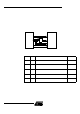
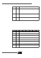
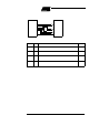
The T89C51AC2 implement 32 Kbytes of on-chip program/code memory. Figure 8
shows t he partitioning of internal and extern al program/ c ode memory spaces dependi ng
on t he product.
The FLASH memory increases EPROM and ROM functionality by in-circuit electrical
erasure and programm ing. Thanks to the internal charge pump, t he high voltage needed
for programming or erasing FLA SH cells is g enerat ed o n-c hip us ing the s t andard VDD
voltage. Thus, the FLASH Mem ory can be program med using only on e voltage and
allows In-System Program ming comm only known as ISP. H ardware programmi ng mo de
is also available using specific pro gramm ing tool.
Figure 8. Program /Code Mem ory Organizat ion
Note: If the program executes exclusively from on-chip code memory (not from external mem-
ory), beware of executing code from t he upper byte of on-chip m emory (7FFFh) and
thereby disrupt I/O Ports 0 and 2 due to external prefetch. Fetching code constant from
this location does not affect Ports 0 and 2.
9.1 External Code
Memory Access
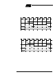
9.1.1 M em ory Interface The external memory interface comprises the external bus (port 0 and port 2) as well as
the bus c ontrol signa ls (PSEN#, and ALE).
Figure 9 shows the structure of the external a ddres s bus . P0 c arries address A 7:0 whil e
P2 c arries address A15:8. Data D7:0 is multiplexe d wi th A 7: 0 on P0 . Table 7 describes
the external mem ory interface signals.
0000h
32 Kbytes
7FFFh
internal
0000h
7FFFh
FFFFh
8000h
FLASH
32 Kbytes
external
memory
32 Kbytes
external
memory
EA = 0
EA = 1