
User Manual


22
T89C51AC2
Rev. B – 19-Dec-01
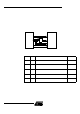
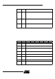
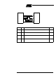
For simplicity, the accompanying figures depict the bus cycle w aveforms in idealized
form and do not provide precise timing information. For bus cycle timing parameters
refer to the Section “AC Characterist ics” of t he T89C5 1A C 2 datasheet.
Figure 5. External Data Read Waveforms
Notes: 1. RD# signal may be stretched using M0 bit in AUXR register.
2. When executing MOVX @Ri instruction, P2 outputs SFR content.
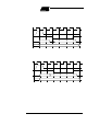
Figure 6. External Data Write Waveforms
Notes: 1. WR# signal may be stretched using M0 bit in AUXR register.
2. When executing MOVX @Ri instruction, P2 outputs SFR content.
ALE
P0
P2
RD#1
DPL or Ri D7:0
DPH or P22
P2
CPU Clock
ALE
P0
P2
WR#1
DPL or Ri D7:0
P2
CPU Clock
DPH or P22