
User Manual

21
T89C51AC2
Rev. B – 19-Dec-01
7.2 External Space
7.2.1 M em ory Interface The external memory interface comprises the external bus (port 0 and port 2) as well as
the bus c ontrol signa ls (RD#, WR#, an d ALE).
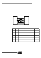
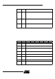
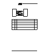
Figure 4 shows the structure of the external a ddres s bus . P0 c arries address A 7:0 whil e
P2 c arries address A15:8. Data D7:0 is multiplexe d wi th A 7: 0 on P0 . Table 2 describes
the external mem ory interface signals.
Figure 4. External Data Memory Interface Structure
Table 2. Ex t ernal Data Mem ory I nt erface Signals
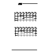
7.2.2 External Bus Cyc les This section describes t he bus cycles the T89C51AC2 execut es to read (see Figure 5),
and write data (see Figure 6) in the ex terna l data memory.
External m emory cycle takes 6 C PU clock periods. This is equivalent to 12 oscillator
clock period in s tandard mode o r 6 oscillator clock pe riods in X2 mode. For further infor-
mation on X2 mode.
Slow peripherals ca n be ac c es sed by stretching the read and w rite cycles. This is done
using the M0 bit in AUXR register. Setting this bit changes the width of the RD# and
WR # signals from 3 to 15 CPU clock periods.
RAM
PERIPHERAL
T89C51AC2
P2
P0
AD7:0
A15:8
A7:0
A15:8
D7:0
A7:0
ALE
WR
OERD#
WR#
Latch
Signal
Name Type Description
Alternative
Function
A15:8 O
Address Lines
Upper address lines for the external bus.
P2.7:0
AD7:0 I/O
Address/Data Lines
Multiplexed lower address lines and data for the external
memory.
P0.7:0
ALE O
Address Latch Enable
ALE signals indicates that valid address information are available
on lines AD7:0.
-
RD# O
Read
Read signal output to external data memory .
P3.7
WR# O
Write
Write signal output to external memory .
P3.6