
User Manual

20
T89C51AC2
Rev. B – 19-Dec-01
7.1 Internal Space
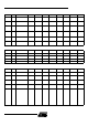
7.1.1 Lower 128 Bytes RAM The lower 128 bytes of RA M (see Figure 2) are accessible f rom address 00h to 7Fh
using direct or indi re ct addressing modes. The lowest 32 bytes are grouped into 4 banks
of 8 registers (R0 to R7). Two bits RS 0 and RS1 in PSW register (see Fig ure 3) select
which bank is in use according to Table 1. This allows m ore efficient use of code space,
sinc e reg ister inst ruc tions are shorter than instr uc tions that use direct addressing, and
can be used for context s witching in interrupt serv ice routines.
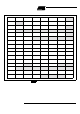
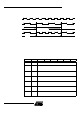
Table 1. Registe r B ank Selection
The next 16 bytes above the register banks form a block of bit-addressable mem ory
space. The C 51 instruction s et in cludes a wide se lect ion of singl e-bit ins tructions, and
the 128 bits in this area can be directly addressed by these instructions. The bit
addres se s in this a rea are 00h t o 7Fh.
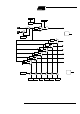
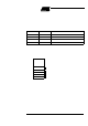
Figure 3. Lower 128 bytes I nternal RAM Organiz ation
7.1.2 Upper 128 Bytes RAM The upper 128 bytes of RAM are accessibl e from address 80h to FFh using o nly indirect
addres sing mod e.
7.1.3 Expanded RAM The on-chip 1024 by t es of expanded RAM (ERAM) are acc ess ible from address 0000h
to 03FFh using indirect addressing mode through MOVX instruc tions. I n t his address
range, the bit EXTRAM in AUXR register is used to select the ERAM (default) or the
XR AM . As s hown in Fig ure 2 when E XTRA M= 0 , the E RAM is s ele cte d a nd when
EXTRAM= 1, t he XRAM i s s elected.
The size of E RAM c an be configured by XRS1-0 bit in AUXR register (default s ize is
1024 bytes).
Note: Lower 128 bytes RAM, Upper 128 b ytes RAM, and expanded RAM are made of volatile
memory cells. This means that the RAM content is indeterminate after power-up and
must then be ini tialized properly.
RS1 RS0 Description
0 0 Register bank 0 from 00h to 07h
0 1 Register bank 0 from 08h to 0Fh
1 0 Register bank 0 from 10h to 17h
1 1 Register bank 0 from 18h to 1Fh
Bit-Addressable Space
4 Banks of
8Registers
R0-R7
30h
7Fh
(Bit Addresses 0-7Fh)
20h
2Fh
18h
1Fh
10h
17h
08h
0Fh
00h
07h