
Instruction Manual

31
T5760/T5761
4561B–RKE–10/02
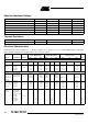
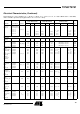
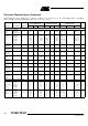
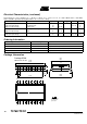
Electrical Characteristics (continued)
All parameters refer to GND, T
amb
= -40°C to +105°C, V
S
= 4.5 V to 5.5 V, f
0
= 868.3 MHz and f
0
=915MHz,
unless otherwise specified. (For typical values: V
S
= 5 V, T
amb
= 25°C)
Parameters Test Conditions Symbol Min. Typ. Max. Unit
Current consumption Sleep mode
(XTO and polling logic active)
IS
off
170 276 µA
IC active (start-up-, bit-check-,
receiving mode) Pin DATA = H
FSK
ASK
IS
on
7.8
7.4
9.9
9.6
mA
mA
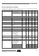
LNA, Mixer, Polyphase Lowpass and IF Amplifier (Input Matched According to Figure 33 Referred to RFIN)
Third-order intercept point LNA/mixer/IF amplifier IIP3 -16 dBm
LO spurious emission Required according to I-ETS 300220 IS
LORF
-70 -57 dBm
System noise figure With power matching |S11| < -10 dB NF 5 dB
LNA_IN input impedance at 868.3 MHz
at 915 MHz
Zi
LNA_IN
200 || 3.2
200 || 3.2
W || pF
W || pF
1 dB compression point IP
1db
-25 dBm
Image rejection Within the complete image band 20 30 dB
Maximum input level BER
£ 10
-3
,
FSK mode
ASK mode
P
in_max
-10
-10
dBm
dBm
Local Oscillator
Operating frequency range VCO T5760
T5761
f
VCO
f
VCO
866
900
871
929
MHz
MHz
Phase noise local oscillator f
osc
= 867.3 MHz at 10 MHz L (fm) -140 -130 dBC/Hz
Spurious of the VCO at ±f
XTO
-55 -45 dBC
XTO pulling XTO pulling,
appropriate load capacitance must
be connected to XTAL,
crystal C
M
= 7 fF
f
XTAL
= 6.77617 MHz (EU)
f
XTAL
= 7.14063 MHz (US)
f
XTO
-30ppm f
XTAL
+30ppm MHz
Series resonance resistor of the
crystal
Parameter of the supplied crystal
R
S
120 W
Static capacitance at Pin XTAL to
GND
Parameter of the supplied crystal
and board parasitics
C
0
6.5 pF
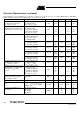
Analog Signal Processing (Input Matched According to Figure 33 Referred to RFIN)
Input sensitivity ASK ASK (level of carrier)
BER
£ 10
-3
, 100% Mod
f
in
= 868.3 MHz/915 MHz
V
S
= 5 V, T
amb
= 25°C
f
IF
= 950 kHz/1 MHz
P
Ref_ASK
BR_Range0 -110 -112 -114 dBm
BR_Range1 -108.5 -110.5 -112.5 dBm
BR_Range2 -108 -110 -112 dBm
BR_Range3 -106 -108 -110 dBm