
Instruction Manual

3
T5760/T5761
4561B–RKE–10/02
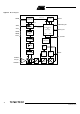
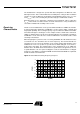
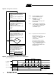
Pin Configuration
Figure 3. Pinning SO20
1
2
3
4
5
6
7
8
10
9
19
18
17
16
14
15
13
12
11
20
AVCC
TEST 1
AGND
n.c.
LNAREF
LNA_IN
IC_ACTIVE
CDEM
DATA_CLK
TEST 4
XTAL
n.c.
TEST 3
POLLING/_ON
DGND
LNAGND
TEST 2
DATA
DVCC
SENS
T5760/
T5761
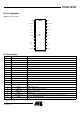
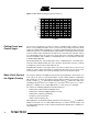
Pin Description
Pin Symbol Function
1 SENS Sensitivity-control resistor
2 IC_ACTIVE IC condition indicator: Low = sleep mode, High = active mode
3 CDEM Lower cut-off frequency data filter
4 AVCC Analog power supply
5 TEST 1 Test pin, during operation at GND
6 AGND Analog ground
7 n.c. Not connected, connect to GND
8 LNAREF High-frequency reference node LNA and mixer
9 LNA_IN RF input
10 LNAGND DC ground LNA and mixer
11 TEST 2 Do not connect during operating
12 TEST 3 Test pin, during operation at GND
13 n.c. Not connected, connect to GND
14 XTAL Crystal oscillator XTAL connection
15 DVCC Digital power supply
16 TEST 4 Test pin, during operation at DVCC
17 DATA_CLK Bit clock of data stream
18 DGND Digital ground
19 POLLING/_ON Selects polling or receiving mode; Low: receiving mode, High: polling mode
20 DATA Data output/configuration input