
Instruction Manual

28
T5760/T5761
4561B–RKE–10/02
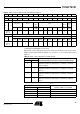
Absolute Maximum Ratings
Parameters Symbol Min. Max. Unit
Supply voltage V
S
6V
Power dissipation P
tot
1000 mW
Junction temperature T
j
150 °C
Storage temperature T
stg
-55 +125 °C
Ambient temperature T
amb
-40 +105 °C
Maximum input level, input matched to 50
W P
in_max
10 dBm
Thermal Resistance
Parameters Symbol Value Unit
Junction ambient R
thJA
100 K/W
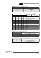
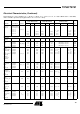
Electrical Characteristics
All parameters refer to GND, T
amb
= -40°C to +105°C, V
S
= 4.5 V to 5.5 V, f
0
= 868.3 MHz and f
0
=915MHz,
unless otherwise specified. (For typical values: V
S
= 5 V, T
amb
= 25°C)
Parameter Test Conditions Symbol
f
RF
= 868.3 MHz
6.77617 MHz Oscillator
f
RF
= 915 MHz
7.14063 MHz Oscillator Variable Oscillator
UnitMin. Typ. Max. Min. Typ. Max. Min. Typ. Max.
Basic Clock Cycle of the Digital Circuitry
Basic clock
cycle
T
Clk
2.0662 2.0662 1.9607 1.9607 14/f
XTO
14/f
XTO
µs
Extended
basic clock
cycle
BR_Range0
BR_Range1
BR_Range2
BR_Range3
T
XClk
16.53
8.26
4.13
2.07
16.53
8.26
4.13
2.07
15.69
7.84
3.92
1.96
15.69
7.84
3.92
1.96
8 ´ T
Clk
4 ´ T
Clk
2 ´ T
Clk
1 ´ T
Clk
8 ´ T
Clk
4 ´ T
Clk
2 ´ T
Clk
1 ´ T
Clk
µs
µs
µs
µs
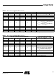
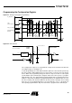
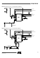
Polling Mode
Sleep time
(see
Figure 11,
Figure 20 and
Figure 33)
Sleep and XSleep
are defined in the
OPMODE register T
Sleep
Sleep ´
X
Sleep
´
1024 ´
2.0662
Sleep ´
X
Sleep
´
1024 ´
2.0662
Sleep ´
X
Sleep
´
1024 ´
1.9607
Sleep ´
X
Sleep
´
1024 ´
1.9607
Sleep ´
X
Sleep
´
1024 ´ T
Clk
Sleep ´
X
Sleep
´
1024 ´ T
Clk
ms
Start-up time
(see
Figure 11 and
Figure 12)
BR_Range0
BR_Range1
BR_Range2
BR_Range3
T
Startup
1852
1059
1059
662
1852
1059
1059
662
1758
1049
1049
628
1758
1049
1049
628
896.5
512.5
512.5
320.5
´ T
Clk
896.5
512.5
512.5
320.5
´ T
Clk
µs
µs
µs
µs
µs
Time for bit
check (see
Figure 11)
Average bit-check
time while polling,
no RF applied
(see Figure 15 and
Figure 16)
BR_Range0
BR_Range1
BR_Range2
BR_Range3
T
Bit-check
0.45
0.24
0.14
0.08
0.45
0.24
0.14
0.08
ms
ms
ms
ms