
Instruction Manual

23
T5760/T5761
4561B–RKE–10/02
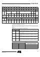
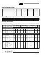
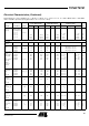
Table 10. Effect of the Configuration Word Lim_min
Note: 1. Lim_min is also used to determine the margins of the data clock control logic (see chapter ’Data Clock’).
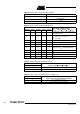
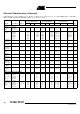
Table 11. Effect of the Configuration Word Lim_max
Note: 1. Lim_max is also used to determine the margins of the data clock control logic (see chapter ’Data Clock’).
Lim_min
(1)
(Lim_min < 10 is not Applicable) Lower Limit Value for Bit Check
Lim_min5 Lim_min4 Lim_min3 Lim_min2 Lim_min1 Lim_min0 (T
Lim_min
= Lim_min × XLim × T
Clk
)
001010 10
001011 11
001100 12
.. .. .. .. .. ..
010101
21 (default)
(T
Lim_min
= 347 µs for f
RF
= 868.3 MHz and
BR_Range0
T
Lim_min
= 329 µs for f
RF
= 915 MHz and
BR_Range0)
.. .. .. .. .. ..
111101 61
111110 62
111111 63
Lim_max
(1)
(Lim_max < 12 is not applicable) Upper Limit Value for Bit Check
Lim_max5 Lim_max4 Lim_max3 Lim_max2 Lim_max1 Lim_max0
(TLim_max = (Lim_max - 1) × XLim ×
T
Clk
)
001100 12
001101 13
001110 14
.. .. .. .. .. ..
101001
41 (default)
(TLim_max = 661 µs for f
RF
= 868.3 MHz
and BR_Range0, TLim_max = 627 µs for
f
RF
= 915 MHz and BR_Range0)
.. .. .. .. .. ..
111101 61
111110 62
111111 63