
Instruction Manual

20
T5760/T5761
4561B–RKE–10/02
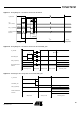
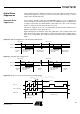
Controlled Noise Suppression by the Microcontroller
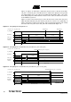
Figure 29. Controlled Noise Suppression
If the bit Noise_Disable (see Table 9) in the OPMODE register is set to 0, digital noise
appears at the end of a valid data stream. To suppress the noise, the Pin
POLLING/_ON must be set to Low. The receiver remains in receiving mode. Then, the
OFF command causes the change to the start-up mode. The programmed sleep time
(see Table 7) will not be executed because the level at Pin POLLING/_ON is low, but
the bit check is active in that case. The OFF command activates the bit check also if the
Pin POLLING/_ON is held to Low. The receiver changes back to receiving mode if the
bit check was successful. To activate the polling mode at the end of the data transmis-
sion, the Pin POLLING/_ON must be set to High. This way of suppressing the noise is
recommended if the data stream is not Manchester or Bi-phase coded.
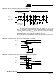
Configuration of the
Receiver
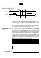
The T5760/T5761 receiver is configured via two 12-bit RAM registers called OPMODE
and LIMIT. The registers can be programmed by means of the bidirectional DATA port.
If the register contents have changed due to a voltage drop, this condition is indicated by
a certain output pattern called reset marker (RM). The receiver must be reprogrammed
in that case. After a Power-On Reset (POR), the registers are set to default mode. If the
receiver is operated in default mode, there is no need to program the registers. Table 3
shows the structure of the registers. According to Table 2, bit 1 defines if the receiver is
set back to polling mode via the OFF command (see chapter ’Receiving Mode’) or if it is
programmed. Bit 2 represents the register address. It selects the appropriate register to
be programmed. To get a high programming reliability, Bit 15 (Stop bit), at the end of the
programming operation, must be set to 0.
Table 1. Effect of Bit 1 and Bit 2 on Programming the Registers
Table 2. Effect of Bit 15 on Programming the Register
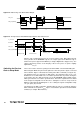
Serial bi-directional
data line
(DATA_CLK)
Preburst Data Digital Noise Preburst Data Digital Noise
Bit check ok Bit check ok
Receiving mode
POLLING/_ON
OFF-command
Receiving mode
Start-up
mode
Bit-check
mode
Sleep
mode
Bit-check
mode
Bit 1 Bit 2 Action
1 x The receiver is set back to polling mode (OFF command)
0 1 The OPMODE register is programmed
0 0 The LIMIT register is programmed
Bit 15 Action
0 The values will be written into the register (OPMODE or LIMIT)
1 The values will not be written into the register