
Instruction Manual

12
T5760/T5761
4561B–RKE–10/02
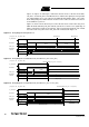
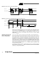
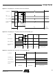
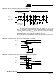
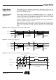
Figure 14, Figure 15 and Figure 16 illustrate the bit check for the bit-check limits
Lim_min = 14 and Lim_max = 24. When the IC is enabled, the signal processing circuits
are enabled during T
Startup
. The output of the ASK/FSK demodulator (Dem_out) is unde-
fined during that period. When the bit check becomes active, the bit-check counter is
clocked with the cycle T
XClk
.
Figure 14 shows how the bit check proceeds if the bit-check counter value CV_Lim is
within the limits defined by Lim_min and Lim_max at the occurrence of a signal edge. In
Figure 15 the bit check fails as the value CV_Lim is lower than the limit Lim_min. The bit
check also fails if CV_Lim reaches Lim_max. This is illustrated in Figure 16.
Figure 11. Timing Diagram During Bit Check
Figure 12. Timing Diagram for Failed Bit Check (Condition: CV_Lim < Lim_min)
Figure 13. Timing Diagram for Failed Bit Check (Condition: CV_Lim >= Lim_max)
Bit check
IC_ACTIVE
Dem_out
Bit-check-
counter
0
2
345
6 245
1
7
8
1
3 6789 111213
14
10
1/2 Bit
15 16
17 18
1
234
56
( Lim_min = 14, Lim_max = 24 )
7891011
12
13
14 15
1234
1/2 Bit 1/2 Bit
Bit check ok
Bit check ok
T
XClk
Start-up mode
Bit-check mode
T
Start-up
T
Bit-check
Bit check
IC_ACTIVE
Bit-check-
counter
0
2345
6 245
1 1
36
789 111210
1/2 Bit
Start-up mode
0
( Lim_min = 14, Lim_max = 24 )
Sleep mode
Bit check failed ( CV_Lim < Lim_min )
Dem_out
Bit-check mode
T
Start-up
T
Bit-check
T
Sleep
Bit check
IC_ACTIVE
Bit-check-
counter
0
23
45
6
2451
7
36
789 111210
1/2 Bit
Start-up mode
20
( Lim_min = 14, Lim_max = 24 )
Sleep mode
Bit check failed ( CV_Lim >= Lim_max )
13 14 15 16
17
18 19 21 22 23 24
0
1
Dem_out
Bit-check mode
T
Start-up
T
Bit-check
T
Sleep