
Owner's manual

2
T5754
4511D–RKE–08/02
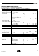
Pin Configuration
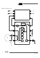
Figure 2. Pinning TSSOP8L
1
2
3
4
8
7
6
5
CLK
PA_ENABLE
ANT2
ANT1
ENABLE
GND
VS
XTAL
T5754
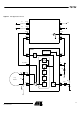
Pin Description
Pin Symbol Function Configuration
1 CLK Clock output signal for microconroller
The clock output frequency is set by the
crystal to f
XTAL
/ 4
2 PA_ENABLE Switches on power amplifier, used for
ASK modulation
3
4
ANT2
ANT1
Emitter of antenna output stage
Open collector antenna output
5 XTAL Connection for crystal
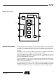
6 VS Supply voltage See ESD protection circuitry (see Figure 8)
7 GND Ground See ESD protection circuitry (see Figure 8)
8 ENABLE Enable input
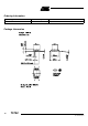
CLK
VS
100
100
PA_ENABLE
50k
Uref=1.1V
20 mA
ANT1
ANT2
XTAL
1.2k
VS
1.5k
VS
182 mA
ENABLE
200k