
Manual
2
T5744
4521A–RKE–02/02
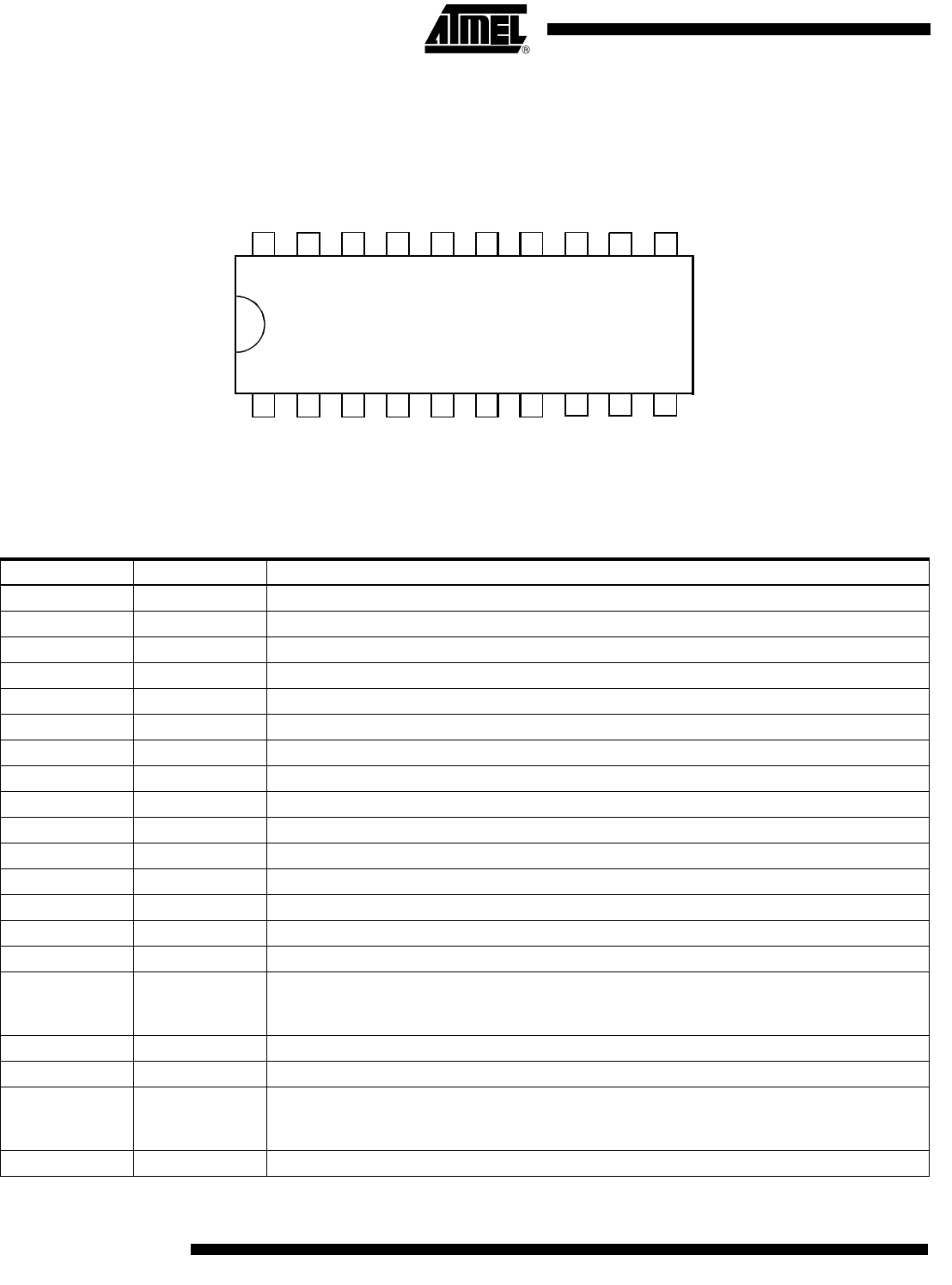
Pin Configuration
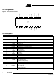
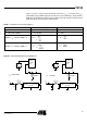
Figure 2. Pinning SO20 and SSO20
Pin Description
Pin Symbol Function
1 BR_0 Baud rate select LSB
2 BR_1 Baud rate select MSB
3 CDEM Lower cut-off frequency data filter
4 AVCC Analog power supply
5 AGND Analog ground
6 DGND Digital ground
7 MIXVCC Power supply mixer
8 LNAGND High-frequency ground LNA and mixer
9LNA_INRF input
10 n.c. Not connected
11 LFVCC Power supply VCO
12 LF Loop filter
13 LFGND Ground VCO
14 XTO Crystal oscillator
15 DVCC Digital power supply
16 MODE
Selecting 433.92 MHz /315 MHz
Low: 315 MHz (USA)
High: 433.92 MHz (Europe)
17 RSSI Output of the RSSI amplifier
18 TEST Test pin, during operation at GND
19 ENABLE
Selecting operation mode
Low: sleep mode
High: receiving mode
20 DATA Data output
1
2
3
4
5
6
7
8
10
9
19
18
17
16
14
15
13
12
11
20
AVCC
AGND
DGND
MIXVCC
LNAGND
LNA_IN
BR_1
CDEM
RSSI
MODE
XTO
LFGND
LF
ENABLE
TEST
n.c.
LFVCC
DATA
DVCC
BR_0
T5744