
Manual

75
T48C862-R4
4551B–4BMCU–02/03
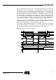
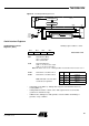
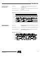
Figure 72. SSI Output Masking Function
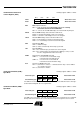
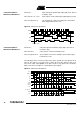
Serial Interface Registers
Serial Interface Control
Register 1 (SIC1)
Auxiliary register address: "9"hex
Note: This bit has to be set to "1" during the MCL mode and the Timer 3 mode 10 or 11
• In Transmit mode (SDD = 1) shifting starts only if the transmit buffer has been
loaded (SRDY = 1).
• Setting SIR-bit loads the contents of the shift register into the receive buffer
(synchronous 8-bit mode only).
• In MCL modes, writing a 0 to SIR generates a start condition and writing a 1
generates a stop condition.
8-bit shift register
MSB LSB
Shift_CL
SO
Control
SI
Timer 2
Output
SSI-control
SO
Compare 2/1
4-bit counter 2/1
CL2/1
SCL
CM1
OMSK
SC
TOG2
POUT
T1OUT
SYSCL
/2
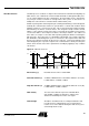
Bit 3Bit 2Bit 1Bit 0
SIR SCD SCS1 SCS0 Reset value: 1111b
SIR Serial Interface Reset
SIR = 1, SSI inactive
SIR = 0, SSI active
SCD Serial Clock Direction
SCD = 1, SC line used as output
SCD = 0, SC line used as input
SCS1 Serial Clock source Select bit 1 SCS1 SCS0 Internal Clock for SSI
SCS0 Serial Clock source Select bit 0 1 1 SYSCL/2
1 0 T1OUT/2
Note: with SCD = 0 the bits SCS1 0 1 POUT/2
and SCS0 are insignificant 0 0 TOG2/2