
Manual

52
T48C862-R4
4551B–4BMCU–02/03
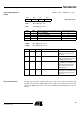
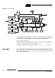
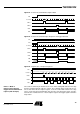
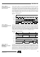
Figure 49. DCG Output Signals
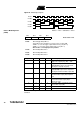
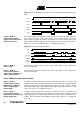
Timer 2 Mode Register 2
(T2M2)
Address: "7"hex - Subaddress: "2"hex
If one of these output modes is used the T2O alternate function of Port 4 must also be
activated.
DCGIN
DCGO0
DCGO1
DCGO2
DCGO3
Bit 3Bit 2Bit 1Bit 0
T2TOP T2OS2 T2OS1 T2OS0 Reset value: 1111b
T2TOP Timer 2 Toggle Output Preset
This bit allows the programmer to preset the Timer 2 output T2O.
T2TOP = 0, resets the toggle outputs with the write cycle (M2 = 0)
T2TOP = 1, sets toggle outputs with the write cycle (M2 = 1)
Note: If T2R = 1, no output preset is possible
T2OS2 Timer 2 Output Select bit 2
T2OS1 Timer 2 Output Select bit 1
T2OS0 Timer 2 Output Select bit 0
Output Mode T2OS2 T2OS1 T2OS0 Clock Output (POUT)
1 1 1 1 Toggle mode: a Timer 2 compare match
toggles the output flip-flop (M2) -> T2O
2 1 1 0 Duty cycle burst generator 1: the DCG output
signal (DCG0) is given to the output and
gated by the output flip-flop (M2)
3 1 0 1 Duty cycle burst generator 2: the DCG output
signal (DCGO) is given to the output and
gated by the SSI internal data output (SO)
4 1 0 0 Biphase modulator: Timer 2 modulates the
SSI internal data output (SO) to Biphase
code
5 0 1 1 Manchester modulator: Timer 2 modulates
the SSI internal data output (SO) to
Manchester code
6 0 1 0 SSI output: T2O is used directly as SSI
internal data output (SO)
7 0 0 1 PWM mode: an 8/12-bit PWM mode
8 0 0 0 Not allowed