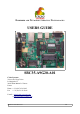
EMBEDDED AND NETWORK COMPUTING TECHNOLOGIES USERS GUIDE SBC35-A9G20-A01 Calao Systems 334 rue des Vingt Toises Le Magistère II 38950 Saint Martin Le Vinoux France Phone = +33 (0)4 76 56 38 05 Fax = +33 (0)4 76 56 38 06 E-mail = sales@calao-systems.com = support@calao-systems.
TABLE OF CONTENTS Section 1...............................................................................................................................................3 1.Overview.......................................................................................................................................3 1.1.Scope.....................................................................................................................................3 1.2.Synoptic..................................
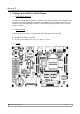
SECTION 1 1. Overview 1.1. Scope The SBC35-A9G20 is a single board computer which runs a full linux environment. It allows to develop applications on a host computer using cross-compilation toolchain and install the results on the SBC35-A9G20. A9G20 board as SBC35-A9G20 This guide focuses on the SBC35-A9G20 an industrial board. The board is equiped with an AT91SAM9G20 processor in an LFBGA217 package. 1.2.
1.3.
SECTION 2 1. Setting Up the SBC35-A9G20 Board 1.1. Electrostatic Warning The SBC35-A9G20 board is shipped in protective anti-static packaging. The board must not be subjected to high electrostatic potentials. A grounding strap or similar protective device should be worn when handling the board. Avoid touching the component pins or any other metallic element. 1.2. Requirements In order to set up the SBC35-A9G20 board, the following items are needed: ● ● the SBC35-A9G20 board itself.
1.4. Powering Up the Board The SBC35-A9G20 requires 5V DC (±5%). DC power is supplied to the board via J3. Coaxial plug center positive standard. 1.5. Getting Started The SBC35-A9G20 board is delivered with a pre-installed U-Boot boot loader and an Embedded Linux operating system. These two components are stored in the NAND Flash. You can update your board by downloading all the available sources and tools on the calao website www.calao-systems.com in order to adapt your system to your needs.
SECTION 3 1.
✔ Based on a Power-on Reset Cell, Reset Source Identification and Reset Output Control Clock Generator (CKGR) ✔ Selectable 32768Hz Low-power Oscillator or Internal Low Power RC Oscillator on Battery Backup Power Supply, Providing a Permanent Slow Clock ✔ 3 to 20 MHz On-chip Oscillator, One up to 800 MHz PLL and One up to 100 MHz PLL Power Management Controller (PMC) ✔ Very Slow Clock Operating Mode, Software Programmable Power Optimization Capabilities ✔ Two Programmable External Clock Signals
✔ ✔ Manchester Encoding/Decoding Support for ISO7816 T0/T1 Smart Card, Hardware Handshaking, RS485 Support Full Modem Signal Control on USART0 Two 2-wire UARTs Two Master/Slave Serial Peripheral Interfaces (SPI) ✔ 8- to 16-bit Programmable Data Length, Four External Peripheral Chip Selects ✔ Synchronous Communications Two Three-channel 16-bit Timer/Counters (TC) ✔ Three External Clock Inputs, Two Multi-purpose I/O Pins per Channel ✔ Double PWM Generation, Capture/Waveform Mode, Up/Down Capabili
1.1. Microcontroller 1x LFBGA 217-ball fitted on board 1.2.
1x 32Kbytes of internal ROM 2x 4Kbytes of internal SRAM 1x 64Kbytes SPI EEPROM memory 1x 64Mbytes of SDRAM memory (32 bits bus width) 1x 256Mbytes of NAND Flash memory (8bits bus width) Bank Start address Size Description Internal memories 0x00000000 256Mbytes EBI CS0 0x10000000 256Mbytes Expansion connectors EBI CS1 (SDRAMC) 0x20000000 64Mbytes Soldered SDRAM EBI CS2 0x30000000 Not available EBI CS3 (NAND) 0x40000000 256Mbytes Soldered NAND Flash EBI CS4 (CF slot 0) 0x500
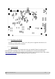
1x Ethernet 100-base TX with three status LED 1.7. User Interface 1x user orange led (LD1) 1x user input pushbutton (SW1) 1.8. Debug Interface 20-pin HE10-2x5 JTAG/ICE interface connector HE10-2x5 DBGU COM Port 1.9. Expansion slot 1x SD/MMC card slot 1x Compact Flash card slot 2x Expansion connectors. These two expansion connectors allow the developer to extend the features of the board by adding external hardware components or boards. SECTION 4 1. Configuration 1.1.
Designation Default setting JP1 1-2 Feature Xin OSC Input level voltage 1-2 : 3.3V 2-3: 1.0V J9 2-3 Slow Clock OSCSEL 1-2: internal RC osc. 2-3: Ext crystal osc. J14 1-2 VDDBU 1-2: Lithium 3V Battery 2-3: 1.
1.2. Memory Memory configuration Designation Default setting Feature R60 Soldered Enables U4 (D[16..31])chip select access R65 Soldered Enables U8 (D[0..15]) chip select access J15 closed Enables the use of NANDFlash R71 Soldered Enables the use of Ready/busy signal S2 Opened Disables write protect SDRAM U4 & U8 NANDFlash U7 1.3. Miscellaneous Designation Default setting Feature R15 soldered USB device: Enables the use of USBCNX signal.
● Pin EBI expansion connector (J11) Description Pin Description 1 D31 2 D30 3 A9 4 A6 5 D29 6 D28 7 A8 8 A7 9 D27 10 D26 11 A11 12 A10 13 D25 14 D24 15 A13 16 A14 17 D23 18 D22 19 D11 20 D10 21 D21 22 D20 23 CFIOW_NBS3_NWR3 24 A1 25 D19 26 D18 27 D13 28 D15 29 D17 30 D16 31 D14 32 D12 33 GND 34 GND 35 CFIOR_NBS1_NWR1 36 D9 37 GND 38 GND 39 D8 40 A2 41 GND 42 GND 43 A3 44 A4 45 GND 46 GND 47 A5 48 A16 49 GND
67 D1 68 D0 69 GND 70 GND 71 A12 72 A15 73 GND 74 GND 75 A20 76 A18 77 GND 78 GND 79 A19 80 A21 81 GND 82 GND 83 PC9/NCS5/CFCS1 84 A22 85 GND 86 GND 87 PC12/IRQ0/NCS7 88 CFWE_NWE_NWR0 89 +3.3V 90 +3.3V 91 CFOE_NRD 92 NCS0 93 +3.3V 94 +3.3V 95 NRST 96 PC15/NWAIT/IRQ1 97 +3.3V 98 +3.3V 99 A0 100 NC ● Pin GPIO expansion connector (J10) Description Pin Description 1 GND 2 GND 3 +3.3V 4 +3.
7 +3.3V 8 +3.
79 GND 80 GND 81 SHDN 82 NC 83 GND 84 GND 85 PB11 86 NC 87 GND 88 GND 89 PB31/PCK1 90 NC 91 GND 92 GND 93 NC 94 NC 95 GND 96 GND 97 NC 98 NC 99 GND 100 GND 1.6. TTL serial port pinout J7, J8, J12 ● Debug Port: J12 Pin Description ● Pin Description 1 NC 2 NC 3 DRXD 4 NC 5 DTXD 6 NC 7 NC 8 NC 9 GND 10 +3.3V COM1 Port: J7 Pin Description Pin Description 1 NC 2 NC 3 RXD1 4 RTS1 5 TXD1 6 CTS1 7 NC 8 NC 9 GND 10 +3.
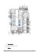
● COM2 Port: J8 Pin Description Pin Description 1 NC 2 NC 3 RXD2 4 RTS2 5 TXD2 6 CTS2 7 NC 8 NC 9 GND 10 +3.3V SECTION 5 1. Schematics 1.1.
Datasheet USG-00019-A01 20/24
Datasheet USG-00019-A01 21/24
Datasheet USG-00019-A01 22/24
Datasheet USG-00019-A01 23/24
SECTION 6 1. Errata SECTION 7 1. Revision History 1.1. Revision History Date Version Remarks 2008-10-10 A01 first version SECTION 8 1. COPYRIGHT Notice: The products specifications provided in this datasheet are subject to change without notice. ©2007 CALAO SYSTEMS-All Rights Reserved. The CALAO SYSTEMS logo is a registered trademark of CALAO SYSTEMS. All other names are the property of their respective owners.