
Owner's manual
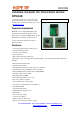


RFM12B
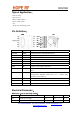
Tel: +86-755-82973806 Fax: +86-755-82973550 E-mail: sales@hoperf.com
http://www.hoperf.com
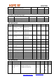
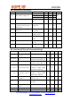
AC characteristic(Transmitter)
symbol parameter remark min typical max Unit
433MHz band 3 5
868MHz band 2 4
P
max
Max. available output power
915MHz band 2 4
dBm
P
out
Typical output power Selectable in 3 dB
steps
P
max
-21 P
max
dbm
C
o
Output capacitance
(set by the automatic antenna
tuning circuit)
In low bands
In high bands
2
2.1
2.6
2.7
3.2
3.3
pf
Q
o
Quality factor of the output
capacitance
In low bands
In high bands
13
8
15
10
17
12
L
out
Output phase noise 100 kHz from carrier
1 MHz from carrier
-80
-103
dbc/HZ
BR
TX
FSK bit rate Via internal TX data
register
172 kbps
BRA
TX
FSK bit rate
TX data connected to the
FSK input
256 kbps
df
fsk
FSK frequency deviation Programmable in 15
kHz steps
15 240 kHZ
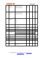
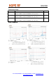
AC characteristic(Turn-on/Turnaround timings)
symbol parameter remark min typical max Unit
T
st
Crystal oscillator
startup time
Crystal ESR < 100 1 5 ms
T
tx_XTAL_ON
Transmitter turn-on
time
Synthesizer off, crystal
oscillator on with 10 MHz step
250 us
T
rx_XTAL_ON
Receiver turn-on time Synthesizer off, crystal
oscillator on with 10 MHz step
250 us
T
tx_rx_SYNT_ON
Transmitter –
Receiver turnover time
Synthesizer and crystal
oscillator on during TX/RX
change with 10 MHz step
150 us
T
rx_tx_SYNT_ON
Receiver –
Transmitter turnover
time
Synthesizer and crystal
oscillator on during RX/TX
change with 10 MHz step
150 us
C
xl
Crystal load
capacitance
Programmable in 0.5 pF steps,
tolerance+/- 10%
8.5 16 pf
t
POR
Internal POR timeout After V
dd
has reached 90% of
final value
100 ms
t
PBt
Wake-up timer clock
period
Calibrated every 30 seconds 0.96 1.05 ms
C
in, D
Digital input apacitance 2 pf
t
r, f
Digital output rise/fall time
15pF pure capacitive load 10 ns