
Manual

RF22
Version: 0.1 Date: 12/23/2008
Tel: +86-755-82973805 Fax: +86-755-82973550 E-mail: sales@hoperf.com http://www.hoperf.com
90
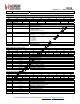
Register 7Fh. FIFO Access
Bit D7 D6 D5 D4 D3 D2 D1 D0
Name fifod[7:0]
Type R/W
Reset value = NA
Bit Name Function
7:0 fifod[7:0] A Write (R/W = 1) to this Address will begin a Burst Write to the TX FIFO.
The FIFO will be loaded in the same manner as a Burst SPI Write but the SPI address will not
be incremented. To conclude the TX FIFO Write the SEL pin should be brought HIGH. A Read
(R/W = 0) to this address will begin a burst read of the RX FIFO, in the same manner.
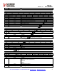
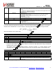
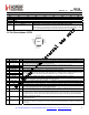
13. Pin Descriptions: RF22
nSEL
nIRO
XOUT
XIN
SON
VDR
GPIO
_2
GPIO
_1
GPIO
_0
ADC
_REF
GND_GID
VR_DIG
SDO
SDI
SCLK
VR_IF
RXn
RXp
TX
VDD_RF
RF22
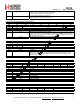
Pin Pin Name I/O Description
1 VDD_RF VDD +1.8 to +3.6 V supply voltage input to all analog +1.7 V regulators. The recommended VDD supply voltage is +3.3 V.
2 TX O Transmit output pin. The maximum level in TX mode is +20 dBm. The PA output is an open-drain connection so the
L-C match must supply VDD (+3.3 VDC nominal) to this pin.
3 RXp I
4 RXn I
Differential RF input pins of the LNA. See application schematic for example matching network.
5 VR_IF O Regulated Output Voltage of the IF 1.7 V Regulator. A 1 µF decoupling capacitor is required.
6 ADC_REF O ADC Reference Voltage Decoupling. A 1 µF decoupling capacitor is required.
7 GPIO_0 I/O
8 GPIO_1 I/O
9 GPIO_2 I/O
General Purpose Digital I/O that may be configured through the registers to perform various functions including:
Microcontroller Clock Output, FIFO status, POR, Wake-Up timer, Low Battery Detect, TRSW, AntDiversity control,
etc. See the SPI GPIO Configuration Registers, Address 0Bh, 0Ch, and 0Dh for more information.
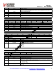
10 VR_DIG O Regulated Output Voltage of the Digital 1.7 V Regulator. A 1 µF decoupling capacitor is required.
11 GND_DIG GND Digital ground supply pin. All analog grounds are connected to the paddle inside the package. The Digital ground is
brought out separately to help isolate the digital and analog domains.
12 VDD_DIG VDD +1.8 to +3.6 V supply voltage input to the Digital +1.7 V Regulator. The recommended VDD supply voltage is +3.3 V.
13 SDO O 0–VDD V digital output that provides a serial readback function of the internal control registers.
14 SDI I Serial Data input pin. 0–VDD V digital input. This pin provides the serial data stream for the 4-line serial data bus.
15 SCLK I Serial Clock input pin. 0–VDD V digital input. This pin provides the serial data clock function for the 4-line serial data
bus. Data is clocked into the RF22 on positive edge transitions.
16 nSEL I Serial Interface Select input pin. 0– VDD V digital input. This pin provides the Select/Enable function for the 4-line
serial data bus. The signal is also used to signify burst read/write mode.
17 nIRQ O General Microcontroller Interrupt Status output pin. When the RF22 exhibits anyone of the Interrupt Events the nIRQ
pin will be set low=0. Please see the Control Logic registers section for more information on the Interrupt Events.
The Microcontroller can then determine the state of the interrupt by reading a corresponding SPI Interrupt Status
Registers, Address 03h and 04h.
18 XOUT O Crystal Oscillator Output. Connect to an external 30 MHz crystal or leave floating if driving the Xin pin with an
external signal source.
19 XIN I Crystal Oscillator Input. Connect to an external 30 MHz crystal or to an external source. If using an external clock
source with no crystal, dc coupling with a nominal 0.8 VDC level is recommended with a minimum ac amplitude of
700 mVpp.