
Manual

RF22
Version: 0.1 Date: 12/23/2008
Tel: +86-755-82973805 Fax: +86-755-82973550 E-mail: sales@hoperf.com http://www.hoperf.com
8
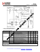
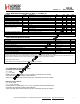
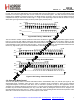
TX Packet
XTAL Settling
Time
0TLLP
LACLLP
S
TLLP
~1ms
PMARAPERP
PUPMARAP
YALEDD
O
MXT
NW
O
DPMARAP
Configurable 0~70us, Default=20us
45us, may be skiped
Configurable 0~310us, Recommended 100us
6us, Fixed
Configurable 5~20us, Recommended 5us
1.5Bits@DR
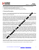
RX Packet
XTAL Settling
Time
0TLLP
LA
C
LLP
S
TLLP
~1ms
Configurable 0~70us, Default=20us
45us, may be skiped
Configurable 0~310us, Recommended 100us
Figure2. TX Timing. Figure3. RX Timing
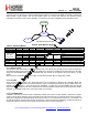
3. Controller Interface
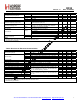
3.1. Serial Peripheral Interface (SPI)
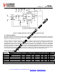
The RF22 communicates with the host MCU over a 3 wire SPI interface: SCLK, SDI, and nSEL. The host MCU can
also read data from internal registers on the SDO output pin. A SPI transaction is a 16-bit sequence which consists of a
Read-Write (R/W) select bit, followed by a 7-bit address field (ADDR), and an 8-bit data field (DATA), as demonstrated
in Figure 4. The 7-bit address field supports reading from or writing to one of the 128, 8-bit control registers. The R/W
select bit determines whether the SPI transaction is a write or read transaction. If R/W = 1, it signifies a WRITE
transaction, while R/W = 0 signifies a READ transaction. The contents (ADDR or DATA) are latched into the RF22
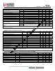
every eight clock cycles. The timing parameters for the SPI interface are shown in Table 10. The SCLK rate is flexible
with a maximum rate of 10 MHz.
Address
Data
RW A5 A3 RW A7A6 xxxxA4 D0A2 A1 A0 D7 D6 D5 D4 D3 D2 D1
LSBMSB
SDI
nSEL
SCLK
Figure4. SPI Timing
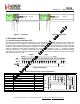
Table10. Serial Interface Timing Parameters
Symbol Parameter Min (nsec) Diagram
t
CH
Clock high time 40
t
CL
Clock low time 40
t
DS
Data setup time 20
t
DH
Data hold time 20
t
DD
Output data delay time 20
t
EN
Output enable time 20
t
DE
Output disable time 50
t
SS
Select setup time 20
t
SH
Select hold time 50
t
SW
Select high period 80
SW
t
DE
t
SH
t
NE
t
SS
t
DD
t
DH
t
DS
t
CH
t
CL
t
nSEL
SCLK
SDI
SDO