
Manual


RF22
Version: 0.1 Date: 12/23/2008
Tel: +86-755-82973805 Fax: +86-755-82973550 E-mail: sales@hoperf.com http://www.hoperf.com
51
11.2. Layout Practice
The following are some general best practice guidelines for PCB layout :
z
Bypass capacitors should be placed as close as possible to the pin.
z TX/RX matching/layout should mimic reference as much as possible. Failing to do so may cause loss in
performance.
z A solid ground plane is required on the backside of the board under TX/RX matching components
z Crystal should be placed as close as possible to the XIN/XOUT pins and should not have VDD traces running
underneath or near it.
z The paddle on the backside of the QFN package needs solid grounding and good soldered connection
z Use GND stitch vias liberally throughout the board, especially underneath the paddle.
11.3. Matching Network Design
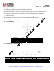
11.3.1. RX LNA Matching
Figure52. RX LNA Matching
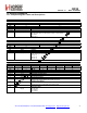
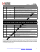
Table 31. RX Matching for Different Bands
Freq Band C1 L C2
915MHz 6.8pF 11.0nH 3.3 pF
868MHz 6.8pF 11.0nH 3.9 pF
433 MHz 10.0 pF 33.0 nH 4.7 pF
315 MHz 15.0 pF 47.0 nH 5.6 pF
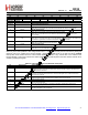
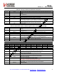
11.3.2. TX PA Matching and Filtering
Freq Band L1 C1 C0 L0 CM LM CM2 LM2 CM3
915 MHz 100.0 nH N/A 22.0 pF 12.0 nH 3.6 pF 18.0 nH 3.0 pF 8.2 nH 0.0 pF
868 MHz 100.0 nH N/A 22.0 pF 12.0 nH 3.3 pF 18.0 nH 2.2 pF 10.0 nH 0.0 pF
433 MHz 120.0 nH 0.4 pF 2.7 pF 47.0 nH 8.2 pF 22.0 nH 13.0 pF 22.0 nH 10.0 pF
315 MHz 150.0 nH 1.0 pF 12.0 pF 33.0 nH 8.2 pF 27.0 nH 8.2 pF 8.2 nH 0.0 pF