
Manual

RF22
Version: 0.1 Date: 12/23/2008
Tel: +86-755-82973805 Fax: +86-755-82973550 E-mail: sales@hoperf.com http://www.hoperf.com
45
30 RFBG RFVREG
31 VCOBG VCOVREG
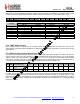
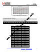
A digital test bus (DTB) is also integrated into the digital portion of the design. The DTB may be configured for output
on the GPIOs. For configuring of the GPIO see registers 0Bh-0Dh. The available digital test points are controlled by the
dtb[4:0] field in "Register 51h. Digital Test Bus Select".
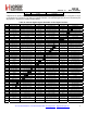
Table 26. Internal Digital Signals Available on the Digital Test Bus
dtb[4:0] GPIO0 Signal GPIO1 Signal GPIO2 Signal
0 wkup_clk_32k wake-up 32 kHz clock rbase_en first divided clock clk_base timebase clock
1 wkup_clk_32k wake-up 32 kHz clock wake_up wake-up event tm1sec 1 sec timebase
2 ts_adc_en aux. ADC enable adc_rdy_n aux. ADC conversion ready adc_done aux. ADC measurement done
3 cont_lbd low battery continuous mode lbd_on low battery ON signal lbd unfiltered output of LBD
4 div_clk_g gated divided clock uc_clk microcontroller clock ckout_rcsel slow clock selected
5 en_div_sync clock divider enable (sync'ed) en_ckout clock out enable en_ckout_s clock out enable (sync'ed)
6 osc30_en oscillator enable osc30_bias2x oscillator bias control xok chip ready
7 xok chip ready
zero_cap
cap. load zero osc30_buff_en buffer enable
8 tsadc_needed aux. ADC enable
ext_retran
ext. retransmission request tx_mod_gpio TX modulation input
9 gpio_0_oen_n GPIO0 output enable gpio_0_aen GPIO0 analog selection gpio_0_aden GPIO0 ADC input line enable
10 int_ack1 interrupt acknowledge 1 int_ack2 interrupt acknowledge 2 int_store interrupt latch closed
11 ext_int2 ext. interrupt from GPIO2 irq_bit8 combined external status msk_bit8 combined masked ext. int.
12 sdo_aux_sel SDO aux. function select sdo_aux SDO aux. signal nirq_aux_sel nIRQ aux. function select
13 trdata_on_sdi TX/RX data on SDI tx_mod TX modulation input tx_clk_out TX clock output
14 start_full_sync RC osc. full calibration start start_fine_sync RC osc. fine calibration
start
xtal_req crystal req. for RC osc. cal.
15 coarse_rdy RC osc. coarse cal. ready fine_rdy RC osc. fine cal. ready xtal_req_sync sync'ed crystal request
16 vco_cal_rst_s_n VCO calibration reset vco_cal VCO calibration is running vco_cal_done VCO calibration done
17 vco_cal_en VCO calibration enable en_ref_cnt reference counter enable en_freq_cnt_s frequency counter enable
18 vco_cal_en VCO calibration enable pos_diff positive difference to goal en_freq_cnt_s frequency counter enable
19 dsm_clk_mux DSM multiplexed clock pll_fb_clk_tst PLL feedback clock pll_ref_clk_tst PLL reference clock
20 dsm[0] delta-sigma output dsm[1] delta-sigma output dsm[2] delta-sigma output
21 dsm[3] delta-sigma output pll_fbdiv15
dsm_rst_s_n delta-sigma reset
22 pll_en PLL enable:TUNE state pllt0_ok PLL initial settling OK pllts_ok PLL soft settling OK
23 ch_freq_req frequency change request pllts_ok PLL soft settling OK vco_cal_done VCO calibration done
24 vco_cal_en VCO calibration enable pll_vbias_shunt_en VCO bias shunt enable
prog_req
frequency recalculation req.
25 bandgap_en bandgap enable frac_div_en fractional divider enable buff3_en buffer3 enable
26 pll_pfd_up PFD up signal pll_pfd_down PFD down signal pfd_up_down PFD output change (XORed)
27 pll_lock_detect PLL lock detect pll_en PLL enable: TUNE state pllt0_ok PLL initial settling OK
28 pll_en PLL enable: TUNE state pll_lock_detect PLL lock detect pllts_ok PLL soft settling OK
29 pwst[0] internal power state pwst[1] internal power state pwst[2] internal power state
30 xok chip ready: READY state pll_en PLL enable: TUNE state
tx_en
TX enable: TX state
31
ts_en
temperature sensor enable
auto_tx_on
automatic TX ON tx_off TX OFF
32 ch_freq_req frequency change request
return_tx
return from TX pk_sent packet sent
33
retran_req
retransmission request tx_ffpt_store TX FIFO pointer store tx_ffpt_restore TX FIFO pointer restore
34 pa_on_trig PA ON trigger dly_5us_ok 5 µs delay expired mod_dly_ok modulator delay expired
35 tx_shdwn TX shutdown
ramp_start
modulator ramp down start ramp_done modulator ramp down ended
36 pk_sent_dly delayed packet sent tx_shdwn_done TX shutdown done
pa_ramp_en
PA ramp enable
37
tx_en
TX enable: TX state ldo_rf_precharge RF LDO precharge
pa_ramp_en
PA ramp enable
38 pa_on_trig TX enable: TX state dp_tx_en packet handler (TX) enable mod_en modulator enable
39
reg_wr_en
register write enable reg_rd_en register rdead enable addr_inc register address increment
40 dp_tx_en packet handler (TX) enable data_start start of TX data pk_sent packet has been sent
41 data_start start of TX data
tx_out
packet handler TX data out pk_sent packet has been sent
42 ramp_done ramp is done data_start start of TX data pk_tx packet is being transmitted
43 tx_ffaf TX FIFO almost full tx_fifo_wr_en TX FIFO write enable tx_ffem_tst internal TX FIFO empty
44 clk_mod modulator gated 10 MHz clock tx_clk TX clock from NCO rd_clk_x8 read clock = tx_clk / 10
45 mod_en modulator enable
ramp_start
start modulator ramping
down
ramp_done modulator ramp done
46 data_start data input start from PH ook_en OOK modulation enble ook OOK modulation