
Manual

RF22
Version: 0.1 Date: 12/23/2008
Tel: +86-755-82973805 Fax: +86-755-82973550 E-mail: sales@hoperf.com http://www.hoperf.com
4
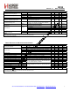
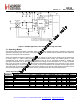
Table4. Transmitter AC Electrical Characteristics
1
Parameter Symbol Conditions Min Typ Max Units
F
SYNTH-LB
Low Band 240 — 480 MHz
TX Frequency Range
2
F
SYNTH-HB
High Band 480 — 930 MHz
FSK Modulation Data Rate
2
DR
FSK
1 — 128 kbps
OOK Modulation Data Rate
2
DR
OOK
1.2 — 40 kbps
Modulation Deviation
2
f ±0.625 ±320 kHz
Modulation Deviation Resolution f
RES
— 0.625 — kHz
Output Power Range
2
P
TX
Tested at 915 MHz, txpow[1:0] = 11 +11 — +20 dBm
TX RF Output Steps
2
P
RF_OUT
TXPWR[1:0] = 00 thru 11 TBD 3 TBD dB
TX RF Output Level Variation vs. Voltage
2
P
RF_V
Measured from VDD=3.6 V to VDD=1.8 V — 2 TBD dB
TX RF Output Level
2
Variation vs. Temperature P
RF_TEMP
–40 to +85
o
C — 2 TBD dB
TX RF Output Level Variation vs. Frequency
2
P
RF_FREQ
Measured across any one frequency band — 1 TBD dB
Transmit Modulation Filtering B*T Gaussian Filtering Bandwith Time Product — 0.5 —
P
OB-TX1
POUT = 11 dBm, Frequencies <1 GHz — — –54 dBm
Spurious Emissions
2
P
OB-TX2
1–12.75 GHz, excluding harmonics — — –54 dBm
P
2HARM
— — –42 dBm
Harmonics
2
P
3HARM
Using Reference Design TX Matching Network
and Filter with Max Output Power (20 dBm).
Harmonics reduce linearly with output power
— — –42 dBm
Notes:
1. All specification guaranteed by production test unless otherwise noted.
2. Guaranteed by qualification.
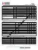
Table5. Auxiliary Block Specifications
1
Parameter Symbol Conditions Min Typ Max Units
Temperature Sensor Accuracy
2
TS
A
When calibrated using temp
sensor offset register
— 0.5 — °C
Temperature Sensor Sensitivity
2
TS
S
— 5 — mV/°C
Low Battery Detector Resolution
2
LBD
RES
— 50 — mV
Low Battery Detector Conversion Time
2
LBD
CT
— 250 — s
Microcontroller Clock Output Frequency
2
MC
Configurable to 30 MHz, 15 MHz, 10 MHz,
4 MHz, 3 MHz, 2 MHz, 1 MHz, or 32.768 kHz
32768 — 30M Hz
General Purpose ADC Accuracy ADC
ENB
— 8 — bit
General Purpose ADC Resolution ADC
RES
— 4 — mV
Temp Sensor & General Purpose ADC Conversion Time ADC
CT
— 305 — sec
30 MHz XTAL Start-Up time t
30M
— 1 — ms
30 MHz XTAL Cap Resolution 30M
RES
— 97 — fF
32 kHz XTAL Start-Up Time t
32k
— 6 — sec
32 kHz XTAL Accuracy 32K
RES
— 100 — ppm
32 kHz RC OSC Accuracy 32KRC
RES
— 2500 — ppm
POR Reset Time t
POR
— 16 — ms
Software Reset Time t
soft
— 100 — s
Notes:
1. All specification guaranteed by production test unless otherwise noted.
2. Guaranteed by qualification.
Table6. Digital IO Specifications (SDO, SDI, SCLK, nSEL, and nIRQ)
Parameter Symbol Conditions Min Typ Max Units
Rise Time T
RISE
0.1 x VDD to 0.9 x VDD, C
L
= 5 pF — — 8 ns
Fall Time T
FALL
0.9 x VDD to 0.1 x VDD, C
L
= 5 pF — — 8 ns
Input Capacitance C
IN
— — 1 pF
Logic High Level Input Voltage V
IH
V
DD
– 0.6 — — V
Logic Low Level Input Voltage V
IL
— 0.6 V
Input Current I
IN
0<V
IN
< V
DD
–100 — 100 nA
Logic High Level Output Voltage V
OH
I
OH
< 1mA source, V
DD
=1.8 V V
DD
– 0.6 — — V
Logic Low Level Output Voltage V
OL
I
OL
<1 mA sink, V
DD
=1.8 V — — 0.6 V
Note: All specification guaranteed by production test unless otherwise noted.