
Manual

RF22
Version: 0.1 Date: 12/23/2008
Tel: +86-755-82973805 Fax: +86-755-82973550 E-mail: sales@hoperf.com http://www.hoperf.com
2
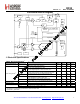
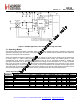
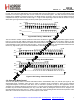
Functional Block Diagram
LPF
CP
Delta Sigma
Modulator
N
LNA
Mixers
PGA
AGC Control
PA
VCO
SPI, & Controller
Digital Logic
PFD
LRT
C
_RWP
TX
RFn
PMAR_AP
PWR_CTRL
PA_RAMP
TXMOD
Digital Modem
Digital LDO
RC 32K OSC
30M XTAL
OSC
RF LDO
IF LDO
VCO LDO
PLL LDO
BIAS
TXRXSW
ANTDIV
Low Power
Digital LDO
POR
Temp
Sensor
SDO
SDI
SCLK
VDD_DIG
VR_IF
LBD
VDD_RF
GND_DIG
8Bit
ADC
RFp
ADC
ADC_REF
GPIO_0
GPIO_1
GPIO_2
VR_DIG
Xin
Xout
VDD_DIG
nSEL
SDN
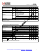
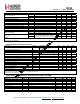
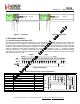
1. Electrical Specifications
Table1. DC Characteristics
1
Parameter Symbol Conditions Min Typ Max Units
Supply Voltage Range V
dd
1.8 3.0 3.6 V
I
Shutdown
RC Oscillator, Main Digital Regulator,
and Low Power Digital Regulator OFF
2
— 10 TBD nA
I
Standby
Low Power Digital Regulator ON (Register values retained)
and Main Digital Regulator, and RC Oscillator OFF
2
— 400 TBD nA
I
Sleep
RC Oscillator and Low Power Digital Regulator ON
(Register values retained) and Main Digital Regulator OFF
2
— 800 TBD nA
I
Sensor-LBD
Main Digital Regulator and Low Battery Detector ON,
Crystal Oscillator and all other blocks OFF
2
— 1 TBD A
I
Sensor-TS
Main Digital Regulator and Temperature Sensor ON,
Crystal Oscillator and all other blocks OFF
2
— 1 TBD A
Power Saving Modes
2
I
Ready
Crystal Oscillator and Main Digital Regulator ON,
all other blocks OFF. Crystal Oscillator buffer disabled
— 600 TBD A
TUNE Mode Current I
Tune
Synthesizer and regulators enabled — 9.5 TBD mA
RX Mode Current I
RX
— 18.5 TBD mA
I
TX_+20
txpow[1:0] = 11 (+20 dBm), VDD = 3.3 V — 60 TBD mA TX Mode Current
I
TX_+11
txpow[1:0] = 00 (+11 dBm), VDD = 3.3 V — 27 TBD mA
Notes:
1. All specification guaranteed by production test unless otherwise noted.
2. Guaranteed by qualification.