
Manual

RF22
Version: 0.1 Date: 12/23/2008
Tel: +86-755-82973805 Fax: +86-755-82973550 E-mail: sales@hoperf.com http://www.hoperf.com
13
setting the vcocal bit. The 32.768 kHz RC oscillator is also automatically calibrated but the calibration may also be
forced. The enrcfcal will enable the RC Fine Calibration which will occur every 30 seconds. The rccal bit will force a
complete calibration of the RC oscillator which will take approximately 2 ms. The PLL T0 time is to allow for bias
settling of the VCO, the default for this should be adequate. The PLL TS time is for the settling time of the PLL, which
has a default setting of 200 s. This setting should be adequate for most applications but may be reduced if small
frequency jumps are used. For more information on the PLL register configuration options, see “Register 53h. PLL
Tune Time,” on page 139 and “Register 55h. Calibration Control,” on page 140.
3.2.9. Frequency Control
For calculating the necessary frequency register settings it is recommended that customers use the easy control
window in HopeRF’s Wireless Design Suite (WDS) or the Excel Calculator available on the product website. These
methods offer a simple method to quickly determine the correct settings based on the application requirements. The
following information can be used to calculate these values manually.
3.2.9.1. Carrier Generation
The carrier frequency is generated by a Fractional-N Synthesizer, using 10 MHz both as the reference frequency and
the clock of the (3
rd order) - modulator. This modulator uses modulo 64000 accumulators. This design was made to
obtain the desired frequency resolution of the synthesizer. The overall division ratio of the feedback loop consist of an
integer part (N) and a fractional part (F). In a generic sense the output frequency of the synthesizer is:
(
)
FNMHf
OUT
+
×
=
10
The fractional part (F) is determined by three different values, Carrier Frequency (fc[15:0]), Frequency Offset (fo[8:0]),
and Frequency Modulation (fd[7:0]). Due to the fine resolution and high loop bandwidth of the synthesizer, FSK
modulation is applied inside the loop and is done by varying F according to the incoming data; this is discussed further
in "3.2.9.4. Frequency Deviation" on page 28. Also, a fixed offset can be added to fine-tune the carrier frequency and
counteract crystal tolerance errors. For simplicity assume that only the fc[15:0] register will determine the fractional
component. The equation for selection of the output frequency is shown below:
(
)
(
)
FNhbselMHzf
TX
+
×
+
×
= 110
()
[]
(
)
⎟
⎠
⎞
⎜
⎝
⎛
++×+×=
64000
]0:15[
240:4110
fc
fbhbselMHzf
TX
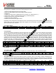
Add R/W Function/Description D7 D6 D5 D4 D3 D2 D1 D0 POR Def.
73 R/W Frequency Offset 1 fo[7] fo[6] fo[5] fo[4] fo[3] fo[2] fo[1] fo[0] 00h
74 R/W Frequency Offset 2 fo[9] fo[8] 00h
75 R/W Frequency Band Select sbsel hbsel fb[4] fb[3] fb[2] fb[1] fb[0] 35h
76 R/W Nominal Carrier Frequency 1 fc[15] fc[14] fc[13] fc[12] fc[11] fc[10] fc[9] fc[8] BBh
77 R/W Nominal Carrier Frequency 0 fc[7] fc[6] fc[5] fc[4] fc[3] fc[2] fc[1] fc[0] 80h
The integer part (N) is determined by fb[4:0]. Additionally, the output frequency can be halved by connecting a ÷2
divider to the output. This divider is not inside the loop and is controlled by the hbsel bit in "Register 75h. Frequency
Band Select". This effectively partitions the entire 240–930 MHz frequency range into two separate bands: High Band
(HB) for hbsel = 1, and Low Band (LB) for hbsel = 0. The valid range of fb[4:0] is from 0 to 23. If a higher value is written
into the register, it will default to a value of 23. The integer part has a fixed offset of 24 added to it as shown in the
formula above. Table 12 demonstrates the selection of fb[4:0] for the corresponding frequency band.
After selection of the fb (N) the fractional component may be solved with the following equation:
[]
()
[]
240:4110
64000
0:15
+×+×
×
=
fbhbselMHz
f
fc
TX
fb and fc are the actual numbers stored in the corresponding registers.