
User Manual

RF12B
Tel: +86-755-86096587 Fax: +86-755-86096602 E-mail: sales@hoperf.com http://www.hoperf.com
GENERAL DEVICE SPECIFICATION
All voltages are referenced to V
ss
, the potential on the ground reference pin VSS.
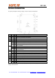
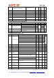
Absolute Maximum Ratings (non-operating)
Symbol Parameter Min Max Units
V
dd
Positive supply voltage -0.5 6 V
V
in
Voltage on any pin (except RF1 and RF2) -0.5 V
dd
+0.5 V
V
oc
Voltage on open collector outputs (RF1, RF2) -0.5
V
dd
+
1
.
5
(
Note 1
)
V
I
in
Input current into any pin except VDD and VSS -25 25 mA
ESD Electrostatic discharge with human body model 1000 V
T
st
Storage temperature -55 125
℃
Recommended Operating Range
Symbol Parameter Min
Max Units
V
dd
Positive supply voltage 2.2
3.8 V
V
ocDC
DC voltage on open collector outputs (RF1, RF2) V
dd
+1.5
V
V
ocAC
AC peak voltage on open collector outputs (RF1, RF2)
V
dd
-1.5
(Note 2)
V
dd
+1 .5
V
T
op
Ambient operating temperature -40
85
℃
Note 1: Cannot be higher than 7 V.
Note 2: Cannot be lower than 1.2 V.
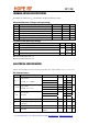
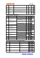
ELECTRICAL SPECIFICATION
(Min/max values are valid over the whole recommended operating range. Typical conditions: T
op
= 27℃; V
dd
=V
oc
=2.7V)
DC Characteristics
Symbol Parameter Conditions/Notes Min Typ Max Units
433 MHz band 15 17
868 MHz band 16 18
I
dd_TX_0
Supply current
(TX mode, P
out
= 0 dBm)
915 MHz band
17 19
mA
433 MHz band 22 24
868 MHz band 23 25 I
dd_TX_PMAX
Supply current
(TX mode, P
out
= P
max
)
915 MHz band 24 26
mA
433 MHz band 11 13
868 MHz band 12 14 I
dd_RX
Supply current
(RX mode)
915 MHz band
13 15
mA
I
pd
Standby current (Sleep mode) All blocks disabled 0.3 µA
I
lb
Low battery voltage detector current
consumption
0.5 µA
I
wt
Wake-up timer current consumption 1.5 µA
I
x
Idle current
Crystal oscillator on
(Note 3)
0.62 1.2 mA