
User Manual

RF12B
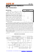
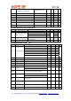
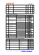
PACKAGE PIN DEFINITIONS
Pin type key: D=digital, A=analog, S=supply, I=input, O=output, IO=input/output
Pin Name Type Function
1 SDI DI Data in
p
ut of the serial control interface
(
SPI com
p
atible
)
2 SCK DI Clock in
p
ut of the serial control interface
3 nSEL DI Chi
p
select in
p
ut of the serial control interface
(
active low
)
4 SDO DO Serial data out
p
ut with bus hold
5 nIRQ DO Interru
p
t re
q
uest out
p
ut
(
active low
)
FSK DI Transmit FSK data in
p
ut
(
internal
p
ull u
p
resistor 133 k
)
DATA DO Received data out
p
ut
(
FIFO not used
)
6
nFFS DI
FIFO select input (active low) In FIFO mode, when bit ef is set in Configuration
Setting Command
DLCK DO Received data clock out
p
ut
(
Di
g
ital filter used, FIFO not used
)
CFIL
A
IO External data filter ca
p
acitor connection
(
Analo
g
filter used
)
7
FFIT DO
FIFO interrupt (active high) Number of the bits in the RX FIFO has reached the
preprogrammed limit
8 CLK DO Microcontroller clock out
p
ut
XTL
A
IO Cr
y
stal connection
(
the other terminal of cr
y
stal to VSS
)
or external reference in
p
ut
9
REF
A
IO External reference input. Use 33 pF series couplin
g
capacito
r
10 nRES DIO O
p
en drain reset out
p
ut with internal
p
ull-u
p
and in
p
ut buffer
(
active low
)
11 VSS S Ground reference volta
g
e
12 RF2
A
IO RF differential si
g
nal in
p
ut/out
p
ut
13 RF1
A
IO RF differential si
g
nal in
p
ut/out
p
ut
14 VDD S Positive su
pp
l
y
volta
g
e
15
A
RSSI
A
O
A
nalo
g
RSSI out
p
ut
nINT DI Interru
p
t in
p
ut
(
active low
)
16
VDI DO Valid data indicator output
Note: The actual mode of the multipurpose pins (pin 6 and 7) is determined by the TX/RX data I/O
settings of the transceiver.
Tel: +86-755-86096587 Fax: +86-755-86096602 E-mail: sales@hoperf.com http://www.hoperf.com